EE 432 Lab 3 PMOS source/drain lithography and diffusion
|
|
|
- Tobias Booth
- 5 years ago
- Views:
Transcription
1 EE 432 Lab 3 PMOS source/drain lithography and diffusion Group Leader: Yue Zhang Group Numbers: Yueyi Jiao, Yin Huang, Lafit Masud TA: Andy Hoyt Section: NO. 5 Introduction: In this lab, we will perform the second lithography step to create the openings needed for the PMOS source and drain regions. Then we will finish the boron diffusion that forms the source and drain regions of the PMOS transistors. The deposition half of the two-step diffusion was done by GT according to the SOPs. We will receive information regarding the soak (deposition) times for our wafers. Overview: The purpose of this lab is to finish the boron diffusion that forms the source and drain regions of the PMOS transistors. Overall, the purpose of the lab is to make sure that the surface concentration of our wafers are 2.5 x 10^18 cm-3 approximately and the junction depth is about 1.25 um.
2 Photolithography The second mask provides the PMOS diffusion pattern that can be used for our final device. It creates the highly doped p-type region in silicon wafer. There are mainly four parts of doing photolithography process. First is the preparation and setup for exposure machine. We first start the vacuum pumping and turn on the nitrogen and air switches of the aligner. Then, we opened the aligner match and pre heat the light bulb which means it could provides the even intensity UV light from the lamp. Then, we placed the mask on the holder by pushing the vacuum mask bottom. When we check the mask is settled on the holder correctly, we put our cleaned wafer aside. The second step is spinning photo resisters on the top of our wafers. We put our wafer in the spinning machine, and drop some HDMS onto the center of the wafer. We spinning our wafer, and after the machine stop by itself, we checked the layer of HDMS and do the same process by replacing HDMS as AZ, which is the photo resistor we need. In this process, once we got a bad result, we use acetone and methanol cleaned the top and repeat spinning process once more, until we reach a good result. Once we finished all of our wafers, we put them in the baking oven and set 88 degree for 25 min. While the 25 min baking is done, it s time to align the wafer and expose the wafer. We turn on the aligner s microscope light, located on the top of the mask aligner. we also choose soft contact mode and focus the microscope on the mask. By open to separation mode, we first rotate the wafer to make its edge parallel with the edge in mask. Then we find a corner on
3 mask and trying to find its corresponding order in the wafer. After we found it, by adjusting the knob for x, y, and z direction, we align the cross mark in mask with the cross marks in wafers together. From the biggest mark down to smallest mark, finally we get to the correct position. We closed the separation mode and checked the exposure time. We put on UV goggles and start to exposure for 90 seconds. Once we finished the exposure, the following step is developing photo resister and post bake. We put some AZ developing solution in the glass pitch dish and put the exposure wafers into pitch dish for about 50 seconds. After the developing is finished, we put the wafer in the holder and put it in water for more than three minutes. We also took pictures of those wafers. We observed that Yue s wafer is not developed enough so we put her wafer in developing solution again for several seconds and wash it again. Finally we saw the good result under microscope.
4 Boron deposition and drive 1. Purpose and Standard Clean The purpose of the standard clean is that didn t let to the chemistry mix and happen the reaction. Moreover, we use the measuring cylinder to measure chemical that the largest amount is 500ml each time. Firstly, we use the measuring cylinder to measure 2500ml DI H2O and put in the SC-1, and the measuring cylinder measure 500ml each time so we need measure five times. We clean the measuring cylinder by DI H2O. Secondly, we use the measuring cylinder to measure 500ml NH4OH and put in the SC-1. We clean the measuring cylinder by DI H2O. Thirdly, we use the measuring cylinder to measure 500ml H2O2 and put in the SC-1. We clean the measuring cylinder by DI H2O. Forth, we use the measuring cylinder to measure 3000ml DI H2O and put in the SC-2, and the measuring cylinder measure 500ml each time so we need measure six times. We clean the measuring cylinder by DI H2O. Fifth, we use the measuring cylinder to measure 500ml HCl and put in the SC-2. We clean the measuring cylinder by DI H2O.
5 Sixth, we use the measuring cylinder to measure 500ml H2O2 and put in the SC-2. We clean the measuring cylinder by DI H2O. Seventh, we waiting the temperature of SC-1 and SC-2 arrive to 80 C and keeping. Eighth, we open the cascade rinse and let the cistern to be full of DI H2O. Ninth, we put the wafers in the mix solution of SC-1 for 15 minutes. Tenth, we put the wafers in the cistern to cascade rinse for 3 minutes. Eleventh, we put the wafers in the HF solution at 15 minutes. Twelfth, we put the wafers in the cistern to cascade rinse for 1 minute. Thirteenth, we put the wafers in the mix solution of SC-2 for 15 minutes. Fourteenth, we put the wafers in the cistern to cascade rinse for 3 minutes. Finally, we use the drying machine to make the wafers to dehydrate. 2. the boron deposition process Figure 1: Shows the initial boron deposition in the p-well regions. Image taken from:
6 The purpose of this portion is to introduce source boron onto the surface of the silicon so that it can be driven in further in the latter drive step (see figure above). For this part of the lab, we essentially performed a P+ dopant diffusion. In our case, the p- type is the Boron, which doped the p-well regions of our wafers. The source wafer was in this case a ceramic wafer of Boron Nitride (BN), which has been oxidized to form surface layers of B 2 O 3 glass. When heated, this B 2 O 3 glass evaporates and condenses on the wafer, leading to the following chemical reaction: After the right amount of Boron has been deposited onto our wafers, we remove the source wafers and continue onto the Boron Drive step to diffuse the boron deeper into the Silicon wafer. To perform the Boron Deposition, we first perform a standard clean. In the next step, we insert our wafers adjacent to BN source wafers on the wafer boat. The wafer boat is then inserted into the furnace at a rate of about 1 inch per 12 seconds. Before inserting the wafers into the furnace, we set the furnace temperature to and the N2 gas flow to be 2 slpm. After the wafers have been inserted into the oven, we bring down the N 2 gas flow to 1 slpm and introduce 1slpm of O 2 gas. This gas flow mixture is continued for 20 minutes. When the 20 minute has passed, we introduce 40 sccm of hydrogen gas into the chamber to begin the sourcing step of the deposition, which takes 2 minutes. When the source step is completed, we perform the main soak step of the deposition. ccording to our calculations shown in the appendix we found that the
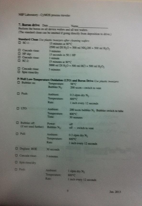
7 soak time should be minutes at a constant temperature of. or this step, we turned off the O 2 and H 2 gasses and introduced 2 lpm of N 2 gas. After the 70 minutes had passed, we pulled out the wafers at a rate of 1 inch per 12 seconds. To finish the deposition steps, we deglazed the wafers in the BOE tub for 30 seconds, followed by rinsing in the cascade rinse tub for 3 minutes and finally spin drying the wafers. 3. the boron drive process, including the LTO Mainly there are three steps of doing boron drive process. By using LTO to remove the boron skin, wet oxidation grows the oxide on silicon wafer and driving process pushing the dopant deeper into the wafer. After we cleaned the wafers, we checked the temperature of tube #3 goes to 800 C, and 1slpm dry N 2 flow. Then we gill the DI water into bubbler and check the bubble goes correctly inside. Then start the nitrogen gas flow through the bubbler with 200 sccm. Then we turn the power to bubbler temperature controller and set temperature of 98 C. We wait for about 15 mins for the heating. We put boron wafers in between of our silicon wafers, and load them into the tube. We push the boat into the center of furnace by using glass rod with the rate of 1 inch every 12 seconds. And we continue do it for totally 5 mins.
8 We checked the bubbler temperature is 98 C, and then turned off the dry N 2 flow. Then we flip the vent bypass switch to tube. And when the oxidation process goes about a half hour, we switch it back, and star to let the N 2 gas flow into the furnace. This is low temperature oxidation (LTO) process. After the LTO process, we are ready to unload our wafers. By using rod with the rate of one inch 12 seconds, we take off our silicon wafers. We put them in the plate and wait them to become cool. We etch the wafers in the BOE tub for 30 seconds and rinse for 3 mins. As usual, we spin to them dry enough. After we spin those wafers, we reload those wafers again it tube #3 with the same rate as before. We checked bubbler as before again and then we turn off the bubbler power and shut off the flow of nitrogen and turn the flow of dry nitrogen to the tube as 1slpm. We check again the temperature is 800 C and then leave our wafers in the furnace overnight ramp tp 600 C and set the nitrogen flow to 0.3 slpm.
9 Results 1. Pattern for PMOS source/drain: For this part, we used a mask level 2 to create a P-type source and drain in N-type well. Comparing to pattern for P-well, in this lab, we need to do alignment since it is essential to avoid making an overlap with P-well. We used microscopy to find a few cross marks in mask as well as in our wafer. By doing this, we can make sure that mask 2 has aligned well with our wafer. After doing the exposure, we took some pictures about our wafer. The picture shows as following: Figures taken in lab: figure 1 figure 2 The cross mark for making alignment After exposure, picture of a part of a die figure 3 Anonther picture of a part of a die
10 figure 4 figure 5 Another cross mark at a different position of wafer A figure shows a part of die firgure 5 Sometime the patter n confuses me. I hope that in class, it may be explained what it is. 2. Problem in this process: 1) During this lab process, the most difficult problem is to how match cross mark in mask and with cross mark in wafer perfectly. Since, we are not familiar with structure of pattern, sometimes we don t know where our wafer is. Even though we found the edge of a die in wafer, it is still a little of difficult to find a right direction to move wafer. 2) Another problem which is not so critical is that during the SiO 2 etch, whether there is water attaching to wafer or not is an important signal for us to stop etching. Sometimes, people forgot to observe this and follow standard operating procedure.
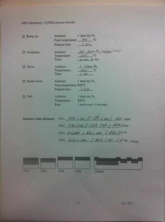
11 3. Boron deposition for PMOS source/drain: For this part, basically, we just did same step in lab for P-well diffusion. There are source and drain well created using boron wafer as a boron source. Professor has done first step in two step diffusion. According to his note, first step is one hour at 850 o C. When we did our lab, we use one hour at 1100 o C. Be careful, in this lab, the time for oxidation should be also taken into account for calculating depth. N(0) Dt Dt dose depth m cm 18 3 cm 13 2 cm 10 2 cm 13 2 Figure2, a profile of P source and drain
12 4. Problem in this process: 1) For this lab, there are not so many problems we met. There are something mentioned for how to control flow of N 2 and H 2 O. Beside, when we need to refill the DI water in bubbler, the TA shows us how to do it correctly in case of break bubbler.
13 Appendix 1. calculation: Constants for Boron Diffusion: EA = 3.50 ev, D0 = 1.0 cm 2 /s NB = 3.25 x cm -3 kb = x 10-5 ev/k T1 = 850 C or 1123 K T2 = 1100 C or 1375 K Diffusion Constants D = D0exp(-EA/kBT) D1 = (1.0)exp(-3.50/(8.617 x 10-5 )(1123)) = x um 2 D2 = (1.0)exp(-3.50/(8.617 x 10-5 )(1375)) = x um 2 t 1 =3600s t 2 =4320s Q 2 N / Dt cm s / / N Q Dt cm 2 x 4 Dt In( N(0) / N ) m j 2 B

14 2. Process Traveler:
15
16
17
18 Conclusion: From this lab, we learn how to perform the second lithography step to create the openings needed for the PMOS source and drain regions. Next we finished the boron diffusion that forms the source and drain regions of the PMOS transistors. Moreover we received information regarding the soak (deposition) times for our wafers.
Photolithography. Operating Instructions
 Photolithography Operating Instructions The PR used during this laboratory session will be Microposit S1813 (from Shipley). Make sure everyone is following the laboratory protocol. Wear lab coats, safety
Equipment Standard Operating Procedure Greg Allion and Kimberly Appel
 Date Created: May 3, 2004 Date Modified: June 1, 2005 MA6/BA6 Mask Aligner Equipment Standard Operating Procedure Greg Allion and Kimberly Appel 1. Purpose 1.1. Photolithography involves transferring a
ABM MASK ALIGNERS. NanoFab 26 March 2009 A Micro Machining & Nanofabrication Facility
 ABM MASK ALIGNERS LOCATION: Optical Lithography PRIMARY TRAINER: Stephanie Bozic (2-6724, sbozic@ualberta.ca) SECONDARY TRAINER: Jolene Chorzempa (2-4823, jolenec@ualberta.ca) 1. OVERVIEW The ABM Mask
VLSI Design I; A. Milenkovic 1
 Switch Model of NMOS Transistor V GS Gate CPE/EE 47, CPE 57 VLSI Design I L0: IC Manufacturing Source (of carriers) Drain (of carriers) Department of Electrical and Computer Engineering University of Alabama
University of Minnesota Nano Fabrication Center
 Equipment name: Karl Suss Mask Aligners Badger name: MA6-P Revision number: 0 Model: MA6 Revisionist: Paul Kimani Location: Bay 4 PAN Date: September 17, 2015 1. Introduction The Karl Suss MA6-PAN is a
Birck Nanotechnology Center
 EFFECTIVE DATE: October 20, 2016 PAGE 1 of 8 This instruction covers the set-up and use of the bench-top for annealing and oxidizing samples within the cleanroom. 1. SAFETY REQUIREMENTS 1.1 Safety glasses
Operation of the contact mask aligner Canon PPC 210 Projection Print Camera
 Operation of the contact mask aligner Canon PPC 210 Projection Print Camera Start-up Procedure: 1. Start the grey pump in the service corridor behind the aligner 2. Open the valve for the Nitrogen gas
CPE/EE 427, CPE 527 VLSI Design I IC Manufacturing. The MOS Transistor
 CPE/EE 427, CPE 527 VLSI Design I IC Manufacturing Department of Electrical and Computer Engineering University of Alabama in Huntsville Aleksandar Milenkovic The MOS Transistor Polysilicon Aluminum 9/11/2006
MJB-3 Mask Aligner Property of TAU MNCF August 2012
 MJB-3 Mask Aligner I. Power Up Sequence 1 LOG IN. Turn on Nitrogen & compressed air lines on the back wall. 2 Turn on the vacuum pump. 3 Flip the COMPRESSED AIR toggle on (up) Compressed air is used to
March CS-1701F Reactive Ion Etcher
 March CS-1701F Reactive Ion Etcher Standard Operating Procedure Faculty Supervisor: Prof. Robert White, Mechanical Engineering (x72210) Safety Office: Peter Nowak x73246 (Just dial this directly on any
COBILT CA-800 Mask Aligner Equipment Operation
 COBILT CA-800 Mask Aligner Equipment Operation For the Micro-Electronics Laboratory At University of Notre Dame Department of Electrical Engineering This user manual is not be removed from room 247A. This
COMELEC C-30-S Parylene Coating System
 COMELEC C-30-S Parylene Coating System Comelec C-30-S Parylene deposition system Introduction Parylene is a polymere deposited at room temperature in a vacuum chamber (few µb). Parylene coating is perfectly
University of Minnesota Nano Fabrication Center Standard Operating Procedure
 Equipment Name: TYLAN Furnace Coral Name: tylan Revision Number: 5 Model: titian Revisionist: Tony Whipple Location: Bay 1 Date: 7 Nov 2006 1 Description The Tylan system is a furnace system for oxidation,
CLEANLINESS STANDARD NCPRE tool contamination classification
 Tool Identifier NCPRE Phosphorous diffusion furnace Document version 1.0 24 th May 2013 Documented by Karthick Murukesan CONTENTS I. CLEANLINESS STANDARD 1 II. PERFOMANCE OF THE TOOL 1 III. WAFER PRE REQUISITE
Usage Policies Notebook for Thermco Atmospheric Diffusion Furnace system
 Usage Policies Notebook for Thermco Atmospheric Diffusion Furnace system Revision date September 2014 2 Emergency Plan for Diffusion Furnaces Standard Operating Procedures for Emergencies Contact information
MJB4 Mask Aligner Operating Procedure. Effective Date: 07/12/2012 Author(s): Jiong Hua Phone:
: Jiong Hua Phone:") MJB4 Mask Aligner Operating Procedure Effective Date: 07/12/2012 Author(s): Jiong Hua Phone: 402-472-3773 Email: jhua2@unl.edu 1 1 Introduction 1.1 Key Words Karl Suss MJB4 Mask Aligner, Optical Lithography,
MJB4 Mask Aligner Operating Procedure Effective Date: 07/12/2012 Author(s): Jiong Hua Phone: 402-472-3773 Email: jhua2@unl.edu 1 1 Introduction 1.1 Key Words Karl Suss MJB4 Mask Aligner, Optical Lithography,
Karl Suss MA6 Mask Aligner SOP
 Page 1 of 11 Karl Suss MA6 Mask Aligner SOP Safety UV Exposure: The high energy light produced by the high pressure Mercury Xenon lamp can cause eye damage and skin burns. Be sure that the light guards
Usage Policies Notebook for Xenon Difluoride (XeF 2 ) Isotropic Si Etch
 Isotropic Si Etch") Usage Policies Notebook for Xenon Difluoride (XeF 2 ) Isotropic Si Etch Revision date September 2014 2 Emergency Plan for XeF 2 Si Etcher Standard Operating Procedures for Emergencies Contact information
Usage Policies Notebook for Xenon Difluoride (XeF 2 ) Isotropic Si Etch Revision date September 2014 2 Emergency Plan for XeF 2 Si Etcher Standard Operating Procedures for Emergencies Contact information
University of Minnesota Nano Fabrication Center
 Equipment name: Karl Suss Mask Aligners Badger name: MA6 & Maba6 Revision number: 4 Models: Revisionist: Paul Kimani Location: Bay 2 Date: April 25, 2013 1. Introduction The Karl Suss MA6 and MABA6 are
Approved by Principal Investigator Date: Approved by Super User: Date:
 Approved by Principal Investigator Date: Approved by Super User: Date: Standard Operating Procedure BNC OAI 200 Lithographic Mask Aligner (Aligner 3) Version 2011 June 2 I. Purpose This Standard Operating
Warnings: Notes: Revised: October 5, 2015
 Karl Suss MA6 Mask Aligner Standard Operating Procedure Faculty Supervisor: Prof. Robert White, Mechanical Engineering (x72210) Safety Office: Peter Nowak x73246 (Just dial this directly on any campus
Operation of the mask aligner MJB-55
 John Paul Adrian Glaubitz Operation of the mask aligner MJB-55 Department of Physics Faculty of Mathematics and Natural Sciences University of Oslo 1 Introduction The mask aligner is an essential tool
KARL SUSS MJB3 UV400 Mask Aligner Standard Operating Procedure
 KARL SUSS MJB3 UV400 Mask Aligner Standard Operating Procedure Version: 1.0 February 2014 UNIVERSITY OF TEXAS AT ARLINGTON Nanotechnology Research Center (NRC) 1 TABLE OF CONTENTS 1 Introduction 3 1.1
The MRL Furnaces USED FOR THIS MANUAL COVERS
 The MRL Furnaces USED FOR 1. Making Silicon Oxide films from 10nm to 2um thickness 2. Annealing with temperatures from 30 800C and times from 5min to 2days 3. Diffusion with temperatures from 30 1100C
MINIBRUTE ANNEAL TUBE STANDARD OPERATION PROCEDURE
 Arizona State University NanoFab MINIBRUTE ANNEAL TUBE STANDARD OPERATION PROCEDURE Rev A Title: MINIBRUTE ANNEAL TUBE STANDARD OPERATION PROCEDURE Table of Contents Issue: Rev A Contents Table of Contents...1
Plasma II (AXIC) Standard Operating Procedure. Revision: 1.0 Last Updated: Feb.6/2013, Revised by Grace Li
 Standard Operating Procedure. Revision: 1.0 Last Updated: Feb.6/2013, Revised by Grace Li") Plasma II (AXIC) Standard Operating Procedure Revision: 1.0 Last Updated: Feb.6/2013, Revised by Grace Li Overview This document will provide a detailed operation procedure of the Axic Multimode LF-6 plasma
Plasma II (AXIC) Standard Operating Procedure Revision: 1.0 Last Updated: Feb.6/2013, Revised by Grace Li Overview This document will provide a detailed operation procedure of the Axic Multimode LF-6 plasma
THERMAL EVAPORATION UNIT (for Al evaporation)
") THERMAL EVAPORATION UNIT (for Al evaporation) System Owner: NeerajPanwar 9619507210 panwar.iitr@gmail.com System Operator: 1. Bhimraj Sable 9930189878 bhimrajsable71@gmail.com Authorized User: 1. Ramesh
THERMAL EVAPORATION UNIT (for Al evaporation) System Owner: NeerajPanwar 9619507210 panwar.iitr@gmail.com System Operator: 1. Bhimraj Sable 9930189878 bhimrajsable71@gmail.com Authorized User: 1. Ramesh
Usage Policies Notebook for Karl Suss MA6 Mid / Deep UV Mask Aligner
 Usage Policies Notebook for Karl Suss MA6 Mid / Deep UV Mask Aligner Revision date September 2014 2 Emergency Plan for Karl Suss MA6 Aligner Standard Operating Procedures for Emergencies Contact information
KARL SUSS MJB3 MASK ALIGNER STANDARD OPERATING PROCEDURE
 KARL SUSS MJB3 MASK ALIGNER STANDARD OPERATING PROCEDURE Purpose of this Instrument: This instrument is for patterning photosensitive polymers with UV light. Location: White Hall 410 Cleanroom Primary
Warnings: Notes: Revised: January 8,
 OAI Model 204IR Mask Aligner Standard Operating Procedure Faculty Supervisor: Prof. Robert White, Mechanical Engineering (x72210) Safety Office: Peter Nowak x73246 (Just dial this directly on any campus
APPLICATION NOTES: PROCESS GUIDELINES FOR USING PHOSPHOROUS OXYCHLORIDE AS AN N TYPE SILICON DOPANT
 APPLICATION NOTES: PROCESS GUIDELINES FOR USING PHOSPHOROUS OXYCHLORIDE AS AN N TYPE SILICON DOPANT DESCRIPTION Phosphorus Oxychloride (POCl 3 ) is a liquid Phosphorus source used for diffusion of N type
Xactix XeF2 OPERATION MANUAL
 General Information The Xactix e-1 is a xenon difluoride (XeF 2) isotropic silicon etcher. XeF 2 is a vapor phase etch, which exhibits very high selectivity of silicon to photo-resist, silicon dioxide,
SOP for Karl Suss MJB3 #1 Mask Aligner
 SOP for Karl Suss MJB3 #1 Mask Aligner Rev. 5 (30/11/2016) Safety UV Exposure: The high-energy light produced by the high-pressure Mercury Xenon lamp can cause eye damage and skin burns. Be sure that the
Standard Operating Manual
 Standard Operating Manual Fisher Scientific Isotemp TM Model 281A Vacuum Oven Version 1.1 Page 1 of 9 Contents 1. Picture and Location 2. Process Capabilities 2.1 Cleanliness Standard 2.2 Substrate Size
Standard Operating Manual
 Standard Operating Manual AB-M Mask Aligner Version 1.1 Page 1 of 18 Contents 1. Picture and Location 2. Process Capabilities 2.1 Cleanliness Standard 2.2 Wafer Chuck Selection 2.3 Mask Holder Selection
Thermcraft Tube Furnace General Use
 Page 1 of 9 Thermcraft Tube Furnace General Use The Thermcraft furnace is a general use, 3 zone tube furnace capable of reaching temperatures of 1200 C. The large 6 diameter quartz tube is capable of holding
Approved by Principal Investigator Date: Approved by Super User: Date:
 Approved by Principal Investigator Date: Approved by Super User: Date: Standard Operating Procedure BNC OAI Lithographic Mask Aligner (Aligner 2) Version 2008 October 31 I. Purpose This Standard Operating
KOH Etchant Standard Operating Procedure
 KOH Etchant Standard Operating Procedure Prepared by: Pauline Stevic Date: April 26, 2018 1. Purpose and application Preferential Silicon Etchants are preparations which have the greatest etch rate on
Plasma 1 (Technics) Standard Operating Procedure. Revision: 1.0 Last Updated: Feb.5/2013, Revised by Grace Li
 Standard Operating Procedure. Revision: 1.0 Last Updated: Feb.5/2013, Revised by Grace Li") Plasma 1 (Technics) Standard Operating Procedure Revision: 1.0 Last Updated: Feb.5/2013, Revised by Grace Li Overview This document will provide a detailed operation procedure of the Technics PE II-A plasma
Plasma 1 (Technics) Standard Operating Procedure Revision: 1.0 Last Updated: Feb.5/2013, Revised by Grace Li Overview This document will provide a detailed operation procedure of the Technics PE II-A plasma
STS ICP-RIE. Scott Munro (2-4826,
 STS ICP-RIE LOCATION: Plasma Etch Area PRIMARY TRAINER: Scott Munro (2-4826, email@address.com) 1. OVERVIEW The STS ICP-RIE is available to users who require deep anisotropic silicon etching with near
Douglas Call 4/11/2008 1/5. Ammonia Treatment
 Douglas Call 4/11/2008 1/5 Ammonia Treatment Department: Chemical Engineering Location: Fenske 102 Contact: Zachary Pace Smith BillyPaul Matthew Holbrook zps5000@psu.edu 166 Fenske bmh200@psu.edu 5-9734
NRF Suss Delta 80 Spinner SOP Revision /14/2016 Page 1 of 11. Suss Delta 80 Spinner SOP
 Page 1 of 11 Note: latest updates are blue. Table of Contents Suss Delta 80 Spinner SOP 1.0 Safety 2.0 Quality Controls and Calibration 3.0 Equipment Uses and Restrictions 4.0 Equipment Specifications
Usage Policies Notebook for Trion RIE / ICP Dry Etch
 Usage Policies Notebook for Trion RIE / ICP Dry Etch Revision date September 2014 2 Emergency Plan for Trion RIE/ICP Dry Etch Standard Operating Procedures for Emergencies Contact information Person Lab
Usage Policies Notebook for Parylene Coating System
 Usage Policies Notebook for Parylene Coating System Revision date September 2014 2 Emergency Plan for Parylene Coating System Standard Operating Procedures for Emergencies Contact information Person Lab
Usage Policies Notebook for STS DRIE System
 Usage Policies Notebook for STS DRIE System Revision date September 2014 2 Emergency Plan for STS DRIE System Standard Operating Procedures for Emergencies Contact information Person Lab Manager Director
Karl Suss MJB4 Mask Aligner
 Karl Suss MJB4 Mask Aligner Tool Manager: Yong Sun ( yongs@princeton.edu; Office 8-8234; Cell 609-917-5076 ) Backup: George Watson ( gwatson@princeton.edu; Office 8-4626; Cell 732-996-2713 ) ******************************************************************************
VOLUMETRIC TECHNIQUES
 REVISED 10/14 CHEMISTRY 1101L VOLUMETRIC TECHNIQUES Volume measurements are important in many experimental procedures. Sometimes volume measurements must be exact; other times they can be approximate.
PLASMA ENHANCED CHEMICAL VAPOR DEPOSITION (PECVD) SOP OXFORD PLASMALAB SYSTEM 100
 SOP OXFORD PLASMALAB SYSTEM 100") PLASMA ENHANCED CHEMICAL VAPOR DEPOSITION (PECVD) SOP OXFORD PLASMALAB SYSTEM 100 June 2013 Interface Overview. The Oxford software is divided into 5 main screens. 1) Pump Control page 2) Recipe page 3)
PLASMA ENHANCED CHEMICAL VAPOR DEPOSITION (PECVD) SOP OXFORD PLASMALAB SYSTEM 100 June 2013 Interface Overview. The Oxford software is divided into 5 main screens. 1) Pump Control page 2) Recipe page 3)
Quintel Mask Aligner
 Quintel Mask Aligner (quintel) 1.0 1.0 Title Quintel Q4000 Mask Aligner 2.0 2.0 Purpose The Quintel Q4000 MA (Mask Aligner) is a top and bottom side contact lithography printer with the video-view split
Title: Xactix XeF2 Etcher Semiconductor & Microsystems Fabrication Laboratory Revision: A Rev Date: 03/23/2016
 Approved by: Process Engineer / / / / Equipment Engineer 1 SCOPE The purpose of this document is to detail the use of the Xactix XeF2 Etcher. All users are expected to have read and understood this document.
Nanofabrication Facility: PECVD SOP Rev. 00, April 24
 Author: Charlie Yao & Mario Beaudoin Email: charlieyao@gmail.com; Beaudoin@physics.ubc.ca Phone: 604-822-1853(MB). Purpose This document outlines the standard operation for the Trion Plasma Enhanced Chemical
Unaxis ICP/RIE SOP Revision 8 09/30/16 Page 1 of 5. NRF Unaxis ICP/RIE Etch SOP
 Page 1 of 5 NRF Unaxis ICP/RIE Etch SOP Unaxis Shuttlelock Reactive Ion Etcher with Inductively Coupled Plasma Module. Etch Capabilities: SiO2, Si3N4, Al, dielectrics and other commonly used materials.
Standard Operating Manual
 Standard Operating Manual Karl Suss MA6 Mask Aligner Version 1.1 Page 1 of 24 Contents 1. Picture and Location 2. Process Capabilities 2.1 Cleanliness Standard 2.2 Substrate Size 2.3 Photo Mask Size 2.4
[USING THE VITROBOT April 9, Using the Vitrobot
 Using the Vitrobot The Vitrobot Mk 3 (aka Mark III, Mark 3, etc.) can control both the local temperature and the local humidity during the process of plunge-freezing a grid for cryoem. It does require
OAI Model 200 Tabletop Mask Aligner Portland State University
 OAI Model 200 Tabletop Mask Aligner Portland State University WARNING: This machine exposes users to ultraviolet radiation. Do not touch the lens underneath the lamp hood as it may damage the machine and
Usage Policies Notebook for NanoFurnace Furnace (EasyTube 3000 System)
") Usage Policies Notebook for NanoFurnace Furnace (EasyTube 3000 System) Revision date October 2014 2 Emergency Plan for Nano Furnace Standard Operating Procedures for Emergencies Contact information Person
Usage Policies Notebook for NanoFurnace Furnace (EasyTube 3000 System) Revision date October 2014 2 Emergency Plan for Nano Furnace Standard Operating Procedures for Emergencies Contact information Person
2.830J / 6.780J / ESD.63J Control of Manufacturing Processes (SMA 6303) Spring 2008
 Spring 2008") MIT OpenCourseWare http://ocw.mit.edu 2.830J / 6.780J / ESD.63J Control of Manufacturing Processes (SMA 6303) Spring 2008 For information about citing these materials or our Terms of Use, visit: http://ocw.mit.edu/terms.
MIT OpenCourseWare http://ocw.mit.edu 2.830J / 6.780J / ESD.63J Control of Manufacturing Processes (SMA 6303) Spring 2008 For information about citing these materials or our Terms of Use, visit: http://ocw.mit.edu/terms.
EXERCISE 2: THE VACUUM SYSTEM
 EXERCISE 2: THE VACUUM SYSTEM Because vacuum system techniques are important to all of experimental physics, every undergraduate student should have had some experience in them. This exercise ensures that
SSI Solaris 150 RTA Revision /27/2016 Page 1 of 9. SSI Solaris 150 RTA
 Page 1 of 9 SSI Solaris 150 RTA The Solaris 150 RTA is a rapid thermal annealing system capable of handling sample sizes up to 100mm (4 diameter) or smaller. The system can anneal in N 2 and Forming gas
Experiment 12: MOLAR VOLUME OF AN IDEAL GAS
 Experiment 1: MOLAR VOLUME OF AN IDEAL GAS Purpose: Determine the molar volume of a gas at standard temperature and pressure (STP, 0 C and pressure of 1 atm) Performance Goals: Collect and measure the
Plasma-Therm PECVD. Operating Characteristics. Operating Instructions. Typical Processes. I. Loading. II. Operating
 Plasma-Therm PECVD A PECVD (plasma enhanced chemical vapor deposition) reacts gases in a RF (radio frequency) induced plasma to deposit materials such as silicon dioxide and silicon nitride. This PECVD
Standard Operating Manual
 Standard Operating Manual Oxford Plasmalab 80 Plus Plasma Etcher Page 1 of 24 Contents 1. Picture and Location 2. Process Capabilities 2.1 Cleanliness Standard 2.2 Available Etching Materials 2.3 Performance
Birck Nanotechnology Center
 EFFECTIVE DATE: October 20, 2016 PAGE 1 of 14 This instruction covers the set-up and use of the bench-top Rapid Thermal Annealing (RTA) systems for processing and annealing samples within the cleanroom.
High Aspect Ratio DRIE on the STS ICP-RIE
 High Aspect Ratio DRIE on the STS ICP-RIE Aspect Ratio Dependant Etching (ARDE) is the difference in the etch depth of features with varying areas of silicon. Areas with more open silicon etch faster compared
General Chemistry I Percent Yield of Hydrogen Gas From Magnesium and HCl
 Introduction For chemical reactions involving gases, gas volume measurements provide a convenient means of determining stoichiometric relationships. A gaseous product is collected in a long, thin graduated
Title: Standard Operating Procedure for Dasibi Model 5008 Gas Dilution Calibrator
 Procedure No: SOP-034 Revision No: 1.0 Revised Dec. 29, 2010 Page No.: 1 of 10 1. INTRODUCTION AND SCOPE This procedure is intended to describe the operations of the Dasibi model 5008 calibrator. The Dasibi
acrolein, acetaldehyde and acetone( cm -1 ); methanol (1306 cm -1 ); ethylene (949 cm -1 ); and isoprene (893 cm -1 ).
; methanol (1306 cm -1 ); ethylene (949 cm -1 ); and isoprene (893 cm -1 ).") acrolein, acetaldehyde and acetone(1550 1800 cm -1 ); methanol (1306 cm -1 ); ethylene (949 cm -1 ); and isoprene (893 cm -1 ). 5 Figure 4a 6 Figure 4b Figure 4c 7 Figure 5 Questions in Student Handout
acrolein, acetaldehyde and acetone(1550 1800 cm -1 ); methanol (1306 cm -1 ); ethylene (949 cm -1 ); and isoprene (893 cm -1 ). 5 Figure 4a 6 Figure 4b Figure 4c 7 Figure 5 Questions in Student Handout
Nanofabrication Facility: ECR Etcher SOP Rev. 01b, March 06. Standard Operating Procedure for PlasmaQuest ECR II Etching
 Standard Operating Procedure for PlasmaQuest ECR II Etching Authors: Rev. 00: Al Schmalz, Vighen Pacradouni and Jeff Young, December 21, 1998 Rev. 01: Dr. Andras G. Pattantyus-Abraham, May 24, 2005 Rev.
University of MN, Minnesota Nano Center Standard Operating Procedure
 Equipment name: STS Etcher Badger name: STS Revision number: 3 Model: 320 Revisionist: Paul Kimani Location: Bay 3 Date: 1 October 2013 A. Description The 320 is a manually loaded batch plasma etching
Ammonia Treatment Instructions Page 1 of 5
 Page 1 of 5 Original version by Douglas Call Updated January 21, 2009 by David Jones Department: Chemical Engineering Location: Fenske 102 (access thru room 103) Contact: BP Matthew Holbrook 161 Fenske
Nordiko Metal Sputtering System Standard Operating Procedure
 Nordiko Metal Sputtering System Standard Operating Procedure Specifications : Target Size Gases used in the system Base pressure Sputtering pressure Substrates used Substrate size : 2 inch or 4 inch :
Oerlikon Sputtering Evaporator SOP
 Oerlikon Sputtering Evaporator SOP Short UNT Cleanroom 1. Taking out sample holder from Transport Chamber : Log in FOM to access the software Go to the software and log in with user1 and password user1
STS PECVD Instructions
 STS PECVD Instructions I. Introduction A PECVD (Plasma Enhanced Chemical Vapor Deposition) reacts gases in a RF- (Radio Frequency) - induced plasma to deposit materials such as SiO 2 and Si X N Y. This
University of MN, Minnesota Nano Center Standard Operating Procedure
 Equipment Name: University of MN, Minnesota Nano Center Deep Trench Etcher Badger Name: deeptrench Revision Number: 9 Model: SLR -770 Sofware Version: CORTEX v4.5 Revisionists: Paul Kimani Location: Bay
MIMS PROCEDURES. Updated 10 Sept 2008
 Updated 10 Sept 2008 MIMS PROCEDURES A. OPERATING PROCEDURES...2 1. Tuning...2 Coarse Tuning...2 Fine Tuning...2 Implantation...2 2. Balancing Trolleys...3 3. Procedure for Bringing Up New Cesium Source...4
Properties of Gases Observing Atom Pressure of a Gas Measuring Gas Products of Chemical Inferring Molecule Reactions
 It s a Gas! In a gas, molecules or atoms move constantly and spread far apart. If a gas cannot escape its container, it applies pressure on the container. For example, gas pressure inflates a balloon.
Karl Suss Contact Aligner Operation
 Karl Suss Contact Aligner Operation Roger Robbins 6/31/2008 2 nd ed. 3/12/2009 The University of Texas at Dallas Erik Jonsson Engineering School of Engineering TITLE: Karl Suss Contact Aligner Operation
How To Use Getters and Getter Pumps
 A Journal of Practical and Useful Vacuum Technology From By Phil Danielson How To Use Getters and Getter Pumps Gettering is a vacuum pumping technology that has been with us, in many forms, for almost
Parallel Reactor Standard Operating Procedure THIS SOP IS NOT MEANT TO REPLACE HANDS-ON TRAINING FROM QUALIFIED PERSONNEL!
 Parallel Reactor Standard Operating Procedure THIS SOP IS NOT MEANT TO REPLACE HANDS-ON TRAINING FROM QUALIFIED PERSONNEL! This SOP describes the basic procedure for using the HEL Cat-24 parallel reactor,
Savannah S100 ALD at SCIF, UC Merced Standard operating Procedure
 This document covers the procedure that should be followed for normal operation of the Cambridge NanoTech: Savannah S100 (Atomic Layer Deposition ALD). This tool is design to be used with whole 4inch wafers.
The SPI Sputter Coater Handbook
 The SPI Sputter Coater Handbook Coating of Specimens SPI-Module Sputter Coater with Etch Mode 1. Mount the specimens onto the SEM stub. Keep in mind that many adhesives have high vapor pressure solvents
Philips SAA7118E Multi Standard Video Decoder Process Review
 March 31, 2006 Philips SAA7118E Multi Standard Video Decoder Process Review For comments, questions, or more information about this report, or for any additional technical needs concerning semiconductor
Approved by Principal Investigator Date: Approved by Super User: Date:
 Approved by Principal Investigator Date: Approved by Super User: Date: Standard Operating Procedure BNC Commonwealth Dual Ion Beam Deposition System (CDIBS) Version 2010 February 14 I. Purpose This Standard
1.1 Equipment: substrate, wafer tweezers, metal targets 1.2 Personal Protective Equipment: nitrile gloves, safety glasses 1.
 Nanomaster NSC-3000 DC Magnetron Sputter Tool Standard Operating Procedure Faculty Supervisor: Prof. Robert White, Mechanical Engineering (x72210) Safety Office: Peter Nowak x73246 (Just dial this directly
Read over Techniques #2, 4, 5, 6, and 9 in the Demonstrations of Nine Practical Lab Techniques booklet.
 Practical Assessment 1 includes: Technique #2 - Use of a Pipette Technique #4 Weighing Technique #5 Use of a Bottle-Top Dispenser Technique #6 Gravity Filtration Technique # 9 Rotary Evaporator Student
OPERATING MANUAL LO-CROSS-FLOW CF M
 VA FILTRATION USA 110 Dodd Court American Canyon, CA 94503 Tel : (707) 552 2616 Fax :(707) 552 3871 Web : www.vafiltration.com OPERATING MANUAL LO-CROSS-FLOW CF8-2-200M January, 2017 TECHNICAL SPECIFICATIONS
Plasma Asher: March PX-500 User guide (May-30, 2017)
") Plasma Asher: March PX-500 User guide (May-30, 2017) This is a highly versatile plasma etch tool that can etch using a direct plasma configuration (Oxygen plasma cleaner), a downstream plasma (Remote plasma),
Plasma Asher: March PX-500 User guide (May-30, 2017) This is a highly versatile plasma etch tool that can etch using a direct plasma configuration (Oxygen plasma cleaner), a downstream plasma (Remote plasma),
Before you start sampling, be sure to read
 6. DISSOLVED OXYGEN MONITORING: MONITORING: Using the Titration Method Before you start sampling, be sure to read the following pages to familiarize yourself with the equipment and the procedures that
Basic ICP Operating Procedures
 Center for High Technology Materials 2 February, 2009 University of New Mexico Created by Beth Fuchs Basic ICP Operating Procedures INTRODUCTION: The ICP is an inductively coupled plasma etching system,
GRAVITY PROBE-B GYRO HOUSING LITHOGRAPHY PROCESS
 PO105 July 15,1997 LITH71597.DOC R. Shile GRAVITY PROBE-B GYRO HOUSING LITHOGRAPHY PROCESS Document Revision Record Rev Date ECO No. Pages Affected Description 1. PHOTORESIST APPLICATION EQUIPMENT AND
NNCI ETCH WORKSHOP SI DRIE IN PLASMATHERM DEEP SILICON ETCHER. Usha Raghuram Stanford Nanofabrication Facility Stanford, CA May 25, 2016
 NNCI ETCH WORKSHOP SI DRIE IN PLASMATHERM DEEP SILICON ETCHER Usha Raghuram Stanford Nanofabrication Facility Stanford, CA May 25, 2016 PLASMATHERM DEEP SI ETCHER PROCESS PARAMETERS Process Parameters/
Revised: June 7, 2017
 LC Technologies Thermal Evaporator Standard Operating Procedure Faculty Supervisor: Prof. Robert White, Mechanical Engineering (x72210) Safety Office: Peter Nowak x73246 (Just dial this directly on any
Measuring Carbon Dioxide in Breath
 Measuring Carbon Dioxide in Breath OBJECTIVES 1. Measure the partial pressure of carbon dioxide in your breath 2. Estimate the volume of air you exhale per day 3. Estimate the volume and mass of CO2 you
MANUAL FOR SPTS APS (DIELECTRICS ETCHER)
") MANUAL FOR SPTS APS (DIELECTRICS ETCHER) To be read first: SPTS APS is an etcher dedicated to dielectrics (SiO 2, Si 3 N 4, glass types...). Dielectrics etching in AMS200 is no more CMi standard. AMS200
MANUAL FOR SPTS APS (DIELECTRICS ETCHER) To be read first: SPTS APS is an etcher dedicated to dielectrics (SiO 2, Si 3 N 4, glass types...). Dielectrics etching in AMS200 is no more CMi standard. AMS200
INTRODUCTION TO THE SPECTROPHOTOMETER AND PIPETTING SKILLS
 INTRODUCTION TO THE SPECTROPHOTOMETER AND PIPETTING SKILLS Section A: Intro to the spectrophotometer A commonly used instrument in the analysis of cellular extracts is the Spectrophotometer. Today you
Standard Operating Procedure. For. PVD E-Beam
 P a g e 1 Standard Operating Procedure For PVD E-Beam P a g e 2 Introduction The PVD Electron-Beam Evaporator (E-Beam) thin film deposition machine uses a magnetically guided and collimated stream of electrons
University of MN, Minnesota Nano Center Standard Operating Procedure
 Equipment Name: Image Reversal Oven Badger name: ir-oven Revision #: 2 Model: YES 310 Revisionist: Paul Kimani Location: Bay 2 Date: October 29, 2013 1. Description The Yield Engineering Systems YES-310
Xactix Xenon Difluoride Etcher
 Xactix Xenon Difluoride Etcher 1 Introduction This tool is a Xactix e1 series XeF2 (Xenon Difluoride) based vapor phase etch system for isotropic and selective silicon etching. The XeF2 reaction with silicon
APPLICATION OF A CHANNEL PLATE IN FIELD-ION MICROSCOPY
 R 718 Philips Res. Repts 25, 87-94,1970 APPLICATION OF A CHANNEL PLATE IN FIELD-ION MICROSCOPY by A. van OOSTROM Abstract Further progress has been made in applying a channel-plate image intensifier in
Using the Akta Prime plus October 22, 2012
 Some starting precautions: 1. Vacuum filter all buffers. Removes any large particles/debris that may clog your column De-gases the buffers 2. Clarify lysates first by centrifugation and then filtration