MOSIS LAMBDA DESIGN RULES
|
|
|
- Catherine Brooks
- 5 years ago
- Views:
Transcription
1 MOSIS LAMBDA DESIGN RULES 3 sets of design rules: 1) SCMOS: valid for technologies with 2λ>1 µm 2) SCMOS_SUBM: valid for technologies with 0.25<2λ 1 µm 3) SCMOS_DEEP: valid for technologies with 2λ 0.25 µm
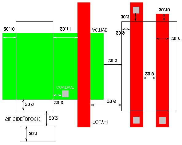
2 LAYOUT DESIGN RULES: an overview Layer GDS CIF CIF Synonym Section N_WELL 42 CWN 1 ACTIVE 43 CAA 2 THICK_ACTIVE 60 CTA 24 Optional POLY 46 CPG 3 SILICIDE_BLOCK 29 CSB 20 Optional N_PLUS_SELECT 45 CSN 4 P_PLUS_SELECT 44 CSP 4 CONTACT 25 CCC CCG 5, 6 Notes POLY_CONTACT 47 CCP 5 Can be replaced by CONTACT ACTIVE_CONTACT 48 CCA 6 Can be replaced by CONTACT METAL1 49 CM1 CMF 7 VIA 50 CV1 CVA 8 METAL2 51 CM2 CMS 9 VIA2 61 CV2 CVS 14 METAL3 62 CM3 CMT 15 VIA3 30 CV3 CVT 21 METAL4 31 CM4 CMQ 22 VIA4 32 CV4 CVQ 25 METAL5 33 CM5 CMP 26 CAP_TOP_METAL 35 CTM 28 Optional VIA5 36 CV5 29 METAL6 37 CM6 30 DEEP_N_WELL 38 CDNW 31 GLASS 52 COG 10 PADS 26 XP Comments -- CX Comments Non-fab layer used to highlight pads
3 SCMOS Layout s - Well SCMOS SUBM DEEP 1.1 Minimum width Minimum spacing between wells at different potential Minimum spacing between wells at same potential Minimum spacing between wells of different type (if both are drawn) 0 0 0
 is illustrated under Select Layout s.")
4 SCMOS Layout s - Active SCMOS SUBM DEEP 2.1 Minimum width 3 * 3 * Minimum spacing Source/drain active to well edge Substrate/well contact active to well edge Minimum spacing between non-abutting active of different implant. Abutting active ("split-active") is illustrated under Select Layout s * Note: For analog and critical digital designs, MOSIS recommends the following minimum MOS channel widths (active under poly) for AMIS designs. Narrower devices, down to design rule minimum, will be functional, but their electrical characteristics will not scale, and their performance is not predictable from MOSIS SPICE parameters. Process Design Technology Design (micrometers) Minimum Width (lambda) AMI_ABN SCNA, SCNE AMI_C5F/N SCN3M, SCN3ME AMI_C5F/N SCN3M_SUBM, SCN3ME_SUBM
5 SCMOS Layout s - Thick Active THICK_ACTIVE is a layer used for those processes offering two different thicknesses of gate oxide (typically for the layout of transistors that operate at two different voltage levels). The ACTIVE layer is used to delineate all the active areas, regardless of gate oxide thickness. THICK_ACTIVE is used to mark those ACTIVE areas that will have the thicker gate oxide; ACTIVE areas outside THICK_ACTIVE will have the thinner gate oxide. THICK_ACTIVE by itself (not covering any ACTIVE polygon) is meaningless. SCMOS SUBM DEEP 24.1 Minimum width Minimum spacing Minimum ACTIVE overlap Minimum space to external ACTIVE Minimum poly width in a THICK_ACTIVE gate Every ACTIVE region is either entirely inside THICK_ACTIVE or entirely outside THICK_ACTIVE

6 SCMOS Layout s - Poly SCMOS SUBM DEEP 3.1 Minimum width Minimum spacing over field a Minimum spacing over active Minimum gate extension of active Minimum active extension of poly Minimum field poly to active 1 1 1
7 SCMOS Layout s - Silicide Block SCMOS SUBM DEEP 20.1 Minimum SB width Minimum SB spacing Minimum spacing, SB to contact (no contacts allowed inside SB) Minimum spacing, SB to external active Minimum spacing, SB to external poly Resistor is poly inside SB; poly ends stick out for contacts the entire resistor must be outside well and over field 20.7 Minimum poly width in resistor Minimum spacing of poly resistors (in a single SB region) Minimum SB overlap of poly or active Minimum poly or active overlap of SB Minimum spacing, SB to poly (in a single active region) NOTE: Some processes do not support both silicide block over active and silicide block over poly. Refer to the individual process description pages.
8

9 SCMOS Layout s - Select 4.1 Minimum select spacing to channel of transistor to ensure adequate source/drain width SCMOS SUBM DEEP Minimum select overlap of active Minimum select overlap of contact Minimum select width and spacing (Note: P-select and N-select may be coincident, but must not overlap) (not illustrated) 2 2 4
, it is required that all features on the insulator layers (CONTACT, VIA, VIA2) must be of the single standard size; there are no exceptions")
10 SCMOS Layout s - Contact to Poly On 0.50 micron process (and all finer feature size processes), it is required that all features on the insulator layers (CONTACT, VIA, VIA2) must be of the single standard size; there are no exceptions for pads (or logos, or anything else); large openings must be replaced by an array of standard sized openings. Contacts must be drawn orthogonal to the grid of the layout. Non- Manhattan contacts are not allowed. If your design cannot tolerate 1.5 lambda contact overlap in 5.2, use the alternative rules which reduce the overlap but increase the spacing to surrounding features. s 5.1, 5.3, and 5.4, still apply and are unchanged. Simple Contact to Poly Alternative Contact to Poly SCMOS SUBM DEEP SCMOS SUBM DEEP 5.1 Exact contact size 2x2 2x2 2x2 5.2.b Minimum poly overlap Minimum poly overlap b Minimum spacing to other poly Minimum contact spacing b Minimum spacing to active (one contact) Minimum spacing to gate of transistor b Minimum spacing to active (many contacts) Simple Poly to Contact

11 Alternative Contact to Poly
12 SCMOS Layout s - Contact to Active If your design cannot handle the 1.5 lambda contact overlap in 6.2, use the alternative rules which reduce the overlap but increase the spacing to surrounding features. s 6.1, 6.3, and 6.4, still apply and are unchanged. Contacts must be drawn orthogonal to the grid of the layout. Non-Manhattan contacts are not allowed. Simple Contact to Active SCMOS SUBM DEEP Alternative Contact to Active SCMOS SUBM DEEP 6.1 Exact contact size 2x2 2x2 2x2 6.2.b Minimum active overlap Minimum active overlap b Minimum spacing to diffusion active Minimum contact spacing b Minimum spacing to field poly (one contact) Minimum spacing to gate of transistor b 6.8.b Minimum spacing to field poly (many contacts) Minimum spacing to poly contact


13 Simple Contact to Active Alternative Contact to Active

14 SCMOS Layout s - Metal1 SCMOS SUBM DEEP 7.1 Minimum width Minimum spacing Minimum overlap of any contact Minimum spacing when either metal line is wider than 10 lambda 4 6 6

15 SCMOS Layout s - Via Vias must be drawn orthogonal to the grid of the layout. Non-Manhattan vias are not allowed. 2 Metal Process 3+ Metal Process SCMOS SUBM DEEP SCMOS SUBM DEEP 8.1 Exact size 2 x 2 n/a n/a 2 x 2 2 x 2 3 x Minimum via1 spacing 3 n/a n/a Minimum overlap by metal1 1 n/a n/a Minimum spacing to contact for technology codes mapped to processes that do not allow stacked vias (SCNA, SCNE, SCN3M, SCN3MLC) 2 n/a n/a 2 2 n/a 8.5 Minimum spacing to poly or active edge 2 n/a n/a 2 2 n/a

16 SCMOS Layout s - Metal2 2 Metal Process 3+ Metal Process SCMOS SUBM DEEP SCMOS SUBM DEEP 9.1 Minimum width 3 n/a n/a Minimum spacing 3 n/a n/a Minimum overlap of via1 1 n/a n/a Minimum spacing when either metal line is wider than 10 lambda 6 n/a n/a 6 6 8

17 SCMOS Layout s - Via2 Vias must be drawn orthogonal to the grid of the layout. Non-Manhattan vias are not allowed. 3 Metal Process 4+ Metal Process SCMOS SUBM DEEP SCMOS SUBM DEEP 14.1 Exact size 2x2 2x2 n/a 2x2 2x2 3x Minimum spacing 3 3 n/a Minimum overlap by metal2 1 1 n/a Minimum spacing to via1 for technology codes that do not allow stacked vias (SCNA, SCNE, SCN3M, SCN3ME, SCN3MLC) 2 2 n/a 2 2 n/a 14.5 Via2 may be placed over contact

18 SCMOS Layout s - Metal3 3 Metal Process 4+ Metal Process SCMOS SUBM DEEP SCMOS SUBM DEEP 15.1 Minimum width 6 5 n/a Minimum spacing to metal3 4 3 n/a Minimum overlap of via2 2 2 n/a Minimum spacing when either metal line is wider than 10 lambda 8 6 n/a 6 6 8

19 SCMOS Layout s - Via3 Vias must be drawn orthogonal to the grid of the layout. Non-Manhattan vias are not allowed. 4 metal Process 5+ Metal Process SCMOS SUBM DEEP SCMOS SUBM DEEP 21.1 Exact size 2x2 2x2 n/a n/a 2x2 3x Minimum spacing 3 3 * n/a n/a Minimum overlap by Metal3 1 1 n/a n/a 1 1 * Exception: Use lambda=4 for rule 21.2 only when using SCN4M_SUBM for Agilent/HP GMOS10QA 0.35 micron process

20 SCMOS Layout s - Metal4 4 Metal Process 5+ Metal Process SCMOS SUBM DEEP SCMOS SUBM DEEP 22.1 METAL4 width 6 6 n/a n/a METAL4 space 6 6 n/a n/a METAL4 overlap of VIA3 2 2 n/a n/a Minimum spacing when either metal line is wider than 10 lambda n/a n/a 6 8
21 SCMOS Layout s - Via4 (SUBM and DEEP) Vias must be drawn orthogonal to the grid of the layout. Non-Manhattan vias are not allowed. 5 Metal Process 6+ Metal Process SCMOS SUBM DEEP SCMOS SUBM DEEP 25.1 Exact size n/a 2x2 3x3 n/a 2x2 3x Minimum spacing n/a 3 3 n/a Minimum overlap by Metal4 n/a 1 1 n/a 1 1
22 SCMOS Layout s - Metal5 (SUBM and DEEP) Any designer using the SCMOS rules who wants the TSMC Thick_Top_Metal must draw the top metal to comply with the TSMC rules for that layer. 5 Metal Process 6+ Metal Process SCMOS SUBM DEEP SCMOS SUBM DEEP 26.1 Minimum width n/a 4 4 n/a Minimum spacing to Metal5 n/a 4 4 n/a Minimum overlap of Via4 n/a 1 2 n/a Minimum spacing when either metal line is wider than 10 lambda n/a 8 8 n/a 6 8
23 SCMOS Layout s - CAP_TOP_METAL for SCMOS_DEEP (and SUBM) The CAP_TOP_METAL layer is used exclusively for the construction of metal-to-metal capacitors. The bottom plate of the capacitor is one of the regular metal layers, as specified below. CAP_TOP_METAL is the upper plate of the capacitor; it is sandwiched physically between the bottom plate metal and the next metal layer above, with a thin dielectric between the bottom plate and the upper (CAP_TOP_METAL) plate. The CAP_TOP_METAL can only be contacted from the metal above; the bottom plate metal can be contacted from below or above (subject, in either case, to rule 28.5), and/or by bottom metal extending outside of the capacitor region (rule 28.7). Use of all (legal) upward vias within that region should be maximized. CAP_TOP_METAL must always be contained entirely within the bottom plate metal. Process Bottom Plate Top Plate Top Plate Contact TSMC_025 METAL4 CAP_TOP_METAL VIA4 and METAL5 TSMC_018 METAL5 CAP_TOP_METAL VIA5 and METAL6 SCMOS SUBM DEEP 28.1 Minimum Width, Capacitor n/a Minimum Spacing (2 capacitors sharing a single bottom plate) Minimum bottom metal overlap (including dummy shapes) n/a n/a Minimum overlap of via n/a Minimum spacing to bottom metal via n/a Minimum bottom metal overlap of its via n/a applicability region extends beyond bottom plate Minimum width, dummy shapes (having no vias) Minimum bottom plate to other bottom plate metal Minimum via separation, on CAP_TOP_METAL Minimum (upward) via separation on bottom metal n/a n/a 4 5 n/a 8 9 n/a n/a 40 45
24 28.12 Maximum CAP_TOP_METAL width and length n/a 30 um Maximum bottom metal plate width and length n/a 35 um No vias from bottom plate downward, directly under top plate CAP_TOP_METAL; dummy metal shapes under capacitor region, discouraged No active or passive circuitry under capacitor region
25 SCMOS Layout s - Via5 (SUBM and DEEP) Vias must be drawn orthogonal to the grid of the layout. Non-Manhattan vias are not allowed. 6 Metal Process SCMOS SUBM DEEP 29.1 Exact size n/a 3 x 3 4 x Minimum spacing n/a Minimum overlap by Metal5 n/a 1 1
26 SCMOS Layout s - Metal6 (SUBM and DEEP) Any designer using the SCMOS rules who wants the TSMC Thick_Top_Metal must draw the top metal to comply with the TSMC rules for that layer. 6 Metal Process SCMOS SUBM DEEP 30.1 Minimum width n/a Minimum spacing to Metal6 n/a Minimum overlap of Via5 n/a Minimum spacing when either metal line is wider than 10 lambda n/a 10 10
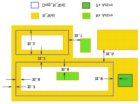
27 SCMOS Layout s - DEEP_N_WELL for SCMOS_DEEP (and SUBM) The DEEP_N_WELL layer provides access to the DNW layer in the TSMC 0.18 and 0.25 processes. This provides a layering sometimes called "triple-well" in which an n-well sits in the p-substrate, and then a p-well sits fully inside of the n-well; it is then possible to construct NMOS devices inside of that isolated p-well. The isolated p-well is surrounded by a fence of standard N_WELL (around its periphery), and by DEEP_N_WELL underneath. The N_WELL fence makes direct electrical contact with the DEEP_N_WELL plate beneath it. DEEP_N_WELL is available in technology codes SCN5M_SUBM, SCN5M_DEEP, SCN6M_SUBM and SCN6M_DEEP but only where these are to be fabricated on TSMC foundry runs. To gain a better understanding of this layer, the TSMC vendor-rule design rule documentation should be studied. SCMOS SUBM DEEP 31.1 Minimum Width, Deep_N_Well n/a Minimum Spacing, Deep_N_Well to Deep_N_Well n/a Minimum extension, N_Well beyond Deep_N_Well edge Minimum overlap, N_Well over Deep_N_Well edge Minimum spacing, Deep_N_Well to unrelated N_Well Minimum spacing, N+Active in isolated P-well, to N_Well Minimum spacing, external N+Active to Deep_N_Well Minimum spacing, P+Active in N_Well to its Deep_N_Well n/a n/a n/a n/a 5 6 n/a n/a 10 13
28

29 SCMOS Layout s - Overglass Note that rules in this section are in units of microns. They are not "true" design rules, but they do make good practice rules. Unfortunately, there are no really good generic pad design rules since pads are process-specific. Microns 10.1 Minimum bonding passivation opening Minimum probe passivation opening Pad metal overlap of passivation Minimum pad spacing to unrelated metal Minimum pad spacing to active, poly or poly2 15
EE 434 Lecture 6. Process Technology
 EE 434 Lecture 6 Process Technology Quiz 4 If an n-channel MOS transistor is modeled with an input capacitance of 2fF and an on resistance of 5KΩ and a p-channel transistor with an input capacitance of
VLSI Design I; A. Milenkovic 1
 Switch Model of NMOS Transistor V GS Gate CPE/EE 47, CPE 57 VLSI Design I L0: IC Manufacturing Source (of carriers) Drain (of carriers) Department of Electrical and Computer Engineering University of Alabama
CPE/EE 427, CPE 527 VLSI Design I IC Manufacturing. The MOS Transistor
 CPE/EE 427, CPE 527 VLSI Design I IC Manufacturing Department of Electrical and Computer Engineering University of Alabama in Huntsville Aleksandar Milenkovic The MOS Transistor Polysilicon Aluminum 9/11/2006
THIẾT KẾ VI MẠCH TƯƠNG TỰ CHƯƠNG 2: CMOS Technology
 THIẾT KẾ VI MẠCH TƯƠNG TỰ CHƯƠNG 2: CMOS Technology Hoàng Trang-bộ môn Kỹ Thuật Điện Tử hoangtrang@hcmut.edu.vn 1 TP.Hồ Chí Minh 12/2011 1. Overview - IC technology - CMOS vs BJT Hoàng Trang-bộ môn Kỹ
ECE520 VLSI Design. Lecture 9: Design Rules. Payman Zarkesh-Ha
 ECE520 VLSI Design Lecture 9: Design Rules Payman Zarkesh-Ha Office: ECE Bldg. 230B Office hours: Wednesday 2:00-3:00PM or by appointment E-mail: pzarkesh@unm.edu Slide: 1 Review of Last Lecture Interconnect
Philips SAA7118E Multi Standard Video Decoder Process Review
 March 31, 2006 Philips SAA7118E Multi Standard Video Decoder Process Review For comments, questions, or more information about this report, or for any additional technical needs concerning semiconductor
STMicroelectronics LISY300AL Single-Axis Analog Yaw Rate Gyroscope
 Single-Axis Analog Yaw Rate Gyroscope MEMS Process Review For comments, questions, or more information about this report, or for any additional technical needs concerning semiconductor technology, please
Freescale Semiconductor MMA6222AEG ±20/20g Dual-Axis Medium-g Micromachined HARMEMS Accelerometer
 Freescale Semiconductor MMA6222AEG ±20/20g Dual-Axis Medium-g Micromachined HARMEMS Accelerometer MEMS Process Review For comments, questions, or more information about this report, or for any additional
Design and Technology Solutions for Development of SiGeMEMS devices. Tom Flynn Vice President, Sales Coventor
 Design and Technology Solutions for Development of SiGeMEMS devices Tom Flynn Vice President, Sales Coventor Special thanks to: Stephane Donnay, Program Manager, imec Gerold Schropfer, Director, Foundary
Layout Design II. Lecture Fall 2003
 Layout Design II Lecture 6 18-322 Fall 2003 Roadmap Today: Layout Verification & design in the large Next week: Transistor sizing Wires Homework 1: Due Today Homework 2: Out Today, Due Sept 18 Lab 2: This
Glass Frit Wafer Bonding Sealed Cavity Pressure in Relation to Bonding Process Parameters. Roy Knechtel, Sophia Dempwolf, Holger Klingner
 10.1149/07509.0255ecst The Electrochemical Society Glass Frit Wafer Bonding Sealed Cavity Pressure in Relation to Bonding Process Parameters Roy Knechtel, Sophia Dempwolf, Holger Klingner X-FAB MEMS Foundry
TOTAL-IONIZING-DOSE RESPONSE OF 65 nm MOSFETS IRRADIATED TO ULTRA- HIGH DOSES. GIULIO BORGHELLO
 TOTAL-IONIZING-DOSE RESPONSE OF 65 nm MOSFETS IRRADIATED TO ULTRA- HIGH DOSES GIULIO BORGHELLO giulio.borghello@cern.ch introduction Presented at NSREC 2017 14/11/2017 GIULIO BORGHELLO 2 introduction Presented
CrimpFlex Crimping Guidelines
 The following guidelines are suggestions to the design engineer and quality control personnel on proven methods of incorporating the CrimpFlex? contact into their designs and into their manufacturing and
Long term stability tests of INO RPC prototypes
 Long term stability tests of INO RPC prototypes While the problem of sudden aging in the glass RPC prototypes is being investigated, a few RPCs of dimension 40 cm 30 cm were fabricated, using glass procured
Manufacturing Processes for WSi 2 -GPSOI Substrates and their Influence on Cross-talk Suppression and Inductance
 Manufacturing Processes for WSi 2 -GPSOI Substrates and their Influence on Cross-talk Suppression and Inductance PT Baine*, HS Gamble *, BM Armstrong *, DW McNeill *, M Bain* J Hamel #, S Stefanos +, M
Leading Edge Logic Comparison. March 9, 2018 Scotten W. Jones President IC Knowledge LLC
 Leading Edge Logic Comparison March 9, 2018 Scotten W. Jones President IC Knowledge LLC sjones@icknowledge.com Logic Standard Cell Logic designs are created using standard cells. The cell height is the
Guidelines to the standard IEC60601
 EUROPEAN POWER SUPPLY MANUFACTURERS ASSOCIATION (Visit the EPSMA website at www.epsma.org) Medical Approvals for Power Supplies Guidelines to the standard IEC60601 Revision Date: 2009-09-12 This document
Experimental Procedure
 1 of 15 9/13/2018, 12:47 PM https://www.sciencebuddies.org/science-fair-projects/project-ideas/sports_p060/sports-science/physics-of-baseball-hit-charts (http://www.sciencebuddies.org/science-fairprojects/project-ideas/sports_p060/sports-science/physics-of-baseball-hit-charts)
CPE/EE 427, CPE 527 VLSI Design I L06: Complementary CMOS Logic Gates
 PE/EE 427, PE 527 VLSI esign I L6: omplementary MOS Logic Gates epartment of Electrical and omputer Engineering University of labama in Huntsville leksandar Milenkovic ( www.ece.uah.edu/~milenka ) www.ece.uah.edu/~milenka/cpe527-5f
New Highly Productive Phased Array Ultrasonic Testing Machine for Aluminium Plates for Aircraft Applications
 19 th World Conference on Non-Destructive Testing 2016 New Highly Productive Phased Array Ultrasonic Testing Machine for Aluminium Plates for Aircraft Applications Christoph HENKEL 1, Markus SPERL 1, Walter
Vacuum Insulation Panels for Buildings and Technical Applications
 Vacuum Insulation Panels for Buildings and Technical Applications Roland Caps va-q-tec AG, Karl-Ferdinand-Braun-Str. 7, D-97080 Würzburg, www.va-q-tec.com ABSTRACT Vacuum insulation panels, which may be
D-PAK Voiding: A Study to Determine the Origins of D-PAK Voiding
 As originally published in the SMTA Proceedings D-PAK Voiding: A Study to Determine the Origins of D-PAK Voiding Kim Flanagan and Greg Wade Indium Corporation Clinton, NY Abstract Voiding in bottom termination
Dissolved Oxygen Guide
 Educat i onser i es Di ssol vedoxygengui de Dissolved Oxygen Guide Introduction Dissolved oxygen probes provide a convenient approach to essentially direct measurement of molecular oxygen. The membrane
RESISTORS, HEATERS, FLEXIBLE, SINGLE AND DOUBLE LAYER. ESCC Detail Specification No. 4009/002
 Page 1 of 16 RESISTORS, HEATERS, FLEXIBLE, SINGLE AND DOUBLE LAYER ESCC Detail Specification Issue 8 February 2018 Document Custodian: European Space Agency see https://escies.org PAGE 2 LEGAL DISCLAIMER
ProChek, A COMPREHENSIVE FABRICATION PROCESS MISMATCH AND RELIABILITY CHARACTERIZATION TOOL
 Vendor: Ridgetop Group, Inc. Office Address: 3580 West Ina Road, Tucson, Arizona 85741 Phone: 520-742-3300; Fax: 520-544-3180 Technical Contact: Esko Mikkola, Ph.D., Project Manager Phone: 520-742-3300
DESIGN AND CHARACTERIZATION OF 20NM SOI MOSFET DOPING ABRUPTNESS DEPENDENT
 DESIGN AND CHARACTERIZATION OF 20NM SOI MOSFET DOPING ABRUPTNESS DEPENDENT A. S. M. Zain 1, N. F. M. Zain 2, F. Salehuddin 1, N. Jamaluddin 2 and N. Abdullah Yaacob 2 1 Centre for Telecommunication Research
Section 2 WHAT DO THE BULBS DO TO MOVING CHARGE?
 Section 2 WHAT DO THE BULBS DO TO MOVING CHARGE? INTRODUCTION We know the filaments of bulbs connected to batteries give off heat and light. We will now investigate how bulb filaments also control the
WBEA Standard Operating Procedure
 Page 1 WBEA Standard Operating Procedure SOP Title Temperature and Relative Humidity Author Gary Cross Implementation date March 2, 2013 Revision History Revision # Date Description Author Page 2 Table
SRI Jigger Tubes System
 SRI Jigger Tubes System Design, Installation and Commissioning Manual (Abbreviated Version) INDEX This manual details how the SRI Jigger Tubes System can be tailored to suit the needs of a variety of vacuum
VLSI Design 14. Memories
 Last module: Synthesis and Verilog This module Memory arrays SRMs Serial Memories Dynamic memories Memory rrays Memory rrays Random ccess Memory Serial ccess Memory Content ddressable Memory (CM) Read/Write
Calibration Procedure. PosiTest DFT Combo
 Management Procedure 2576 Revision: A Date Issued: July 21, 2004 Date Revised: Calibration Procedure DeFelsko Corporation PosiTest DFT Combo Coating Thickness Gages Table of Contents 1 Introduction and
Physical Design of CMOS Integrated Circuits
 Physical Design of CMOS Integrated Circuits Dae Hyun Kim EECS Washington State University References John P. Uyemura, Introduction to VLSI Circuits and Systems, 2002. Chapter 5 Goal Understand how to physically
Tiling And Filling The Pool Student Materials Page 1 of 12
 The Pool Part A At last, your parents have finally agreed that it might be possible to put a small pool in the back yard. The only catch is, your parents are very busy and don t have time to spend figuring
TEPZZ A_T EP A1 (19) (11) EP A1 (12) EUROPEAN PATENT APPLICATION. (51) Int Cl.: G01L 9/00 ( )
 (11) EP A1 (12) EUROPEAN PATENT APPLICATION. (51) Int Cl.: G01L 9/00 ( )") (19) TEPZZ 796844A_T (11) EP 2 796 844 A1 (12) EUROPEAN PATENT APPLICATION (43) Date of publication: 29..2014 Bulletin 2014/44 (51) Int Cl.: G01L 9/00 (2006.01) (21) Application number: 13165416.2 (22)
(19) TEPZZ 796844A_T (11) EP 2 796 844 A1 (12) EUROPEAN PATENT APPLICATION (43) Date of publication: 29..2014 Bulletin 2014/44 (51) Int Cl.: G01L 9/00 (2006.01) (21) Application number: 13165416.2 (22)
EE241 - Spring 2013 Advanced Digital Integrated Circuits. Assigned reading. No new reading. Lecture 4: Transistor Models
 EE41 - Spring 013 Advanced Digital Integrated ircuits ecture 4: Transistor Models Assigned reading No new reading 1 Outline ast lecture Features of modern technologies This lecture Transistor modeling
SMART Pad for CMP. Sunghoon Lee 1, David A. Dornfeld 1 Hae Do Jeong 2. University of California, Berkeley, USA 2
 SMART Pad for CMP Sunghoon Lee 1, David A. Dornfeld 1 Hae Do Jeong 2 1 University of California, Berkeley, USA 2 Pusan National University, Pusan, KOREA Features SMART pad is composed of two stacks of
Influence of HALO and drain-extension doping gradients on transistor performance
 Materials Science and Engineering B 114 115 (2004) 15 19 Influence of HALO and drain-extension doping gradients on transistor performance Axel Erlebach a,, Thomas Feudel b, Andreas Schenk c, Christoph
From Fundamental Detector Research to Industrial Embedded Power Device Technology Development
 From Fundamental Detector Research to Industrial Embedded Power Device Technology Development Joint Instrumentation Seminar DESY, Hamburg University and XFEL Colloquium in honor of Prof. Gunnar Lindström's
Errata CMOS VLSI Design 3 rd Edition
 Errata CMOS VLSI esign 3 rd Edition Last updated 4 September 2006 Send your corrections to bugs@cmosvlsi.com Errata in 2 nd Printing Page viii, Section 4.3: SIzing -> Sizing (N. Ho 8/16/06) Page 39, Table
Equipment Standard Operating Procedure Greg Allion and Kimberly Appel
 Date Created: May 3, 2004 Date Modified: June 1, 2005 MA6/BA6 Mask Aligner Equipment Standard Operating Procedure Greg Allion and Kimberly Appel 1. Purpose 1.1. Photolithography involves transferring a
Applying 3M Graphic Films With Comply Performance
 Instruction Bulletin 5.31 Release D, Effective May 2002 Black bar in margin indicates a change Applying 3M Graphic Films With Comply Performance Table of Contents General Information.....................................
WONDERLAB: THE EQUINOR GALLERY. The science and maths behind the exhibits 30 MIN INFORMATION. Topic FORCES. Age
 WONDERLAB: THE EQUINOR GALLERY and maths s INFORMATION Age 7 11 11 14 Topic FORCES 30 MIN Location LEVEL 3, SCIENCE MUSEUM, LONDON What s the science? What more will you wonder? and maths s Wonderlab:
LiftAlloy Chain Slings
 CHAIN SLING BASICS Slings Lift-All chain slings meet or exceed all OSHA, ASME B30.9 and NACM standards and regulations. chain slings, available in 80 for 7/8"- /4" and 00 for 7/32"-3/4", are recommended
EE 432 Lab 3 PMOS source/drain lithography and diffusion
 EE 432 Lab 3 PMOS source/drain lithography and diffusion Group Leader: Yue Zhang Group Numbers: Yueyi Jiao, Yin Huang, Lafit Masud TA: Andy Hoyt Section: NO. 5 Introduction: In this lab, we will perform
Operating instructions. Surge arrester Type MVR
 Operating instructions Surge arrester Type MVR Content 1 About this document...3 1.1 Validity...3 1.2 Target group...3 2 Safety...3 2.1 Symbols and advices...3 2.2 Basic safety precautions...4 2.2.1 Product
Let it Roll: The Soup Can Experiment
 Let it Roll: The Soup Can Experiment Objectives To roll different kinds of soup cans down a ramp to determine how the content and weight of the can affects how fast and how far it rolls. Materials Procedure
Introduction. Terms of reference. Technical Leaflet T5: The Net Gauge BoD Approval: 2014
 Introduction At present, net gauges are not applicable equipment for approval by ITTF. Nevertheless net gauges have a very important role to keep the matches fair such that: (i) the result of a rally should
38999 Space grade ESA/SCC Section. MIL-DTL Space Grade Circular Connectors
 38999 Space grade ESA/SCC 3401 Section II MI-DT 38999 Space Grade Circular Connectors 59 38999 Space Grade ESA/SCC 3401 Contents 38999 Space Grade ESA/SCC 3401 SCC Specification.......................................................61
VLSI Design 12. Design Styles
 1 9 8 5 1 9 8 7 1 9 9 1 1 9 9 3 1 9 9 9 2 0 0 1 2 0 0 5 2 0 0 7 2 0 0 9 Pr odu ctiv it y (T r an s./ St a f -M o nt h ) VLSI Design Last module: Floorplanning Sequential circuit design Clock skew This
JSP. MKT Series J S P -
 Loose Taped Fig.1 Fig. 2 JSP Typical applications: blocking, coupling, decoupling, by-passing, interference suppression in low voltage applications (i.e.:automotive) Ød ±0.05 All dimensions are in mm.
Total Ionization Dose (TID) Test Results of the RH1028MW Ultralow Noise Precision High Speed Operational Low Dose Rate (LDR)
 Test Results of the RH1028MW Ultralow Noise Precision High Speed Operational Low Dose Rate (LDR)") Total Ionization Dose (TID) Test Results of the RH1028MW Ultralow Noise Precision High Speed Operational Amplifiers @ Low Dose Rate (LDR) LDR = 10 mrads(si)/s 20 February 2015 Duc Nguyen, Sana Rezgui Acknowledgements
Total Ionization Dose (TID) Test Results of the RH1028MW Ultralow Noise Precision High Speed Operational Amplifiers @ Low Dose Rate (LDR) LDR = 10 mrads(si)/s 20 February 2015 Duc Nguyen, Sana Rezgui Acknowledgements
Table of Contents FIRST 2005 FIRST Robotics Competition Manual: Section 3 The Arena rev B Page 1 of 8
 Table of Contents 3 THE ARENA...2 3.1 OVERVIEW...2 3.1.1 Dimensions and Tolerances...3 3.2 PLAYING FIELD...4 3.2.1 Boundaries and Markings...4 3.2.2 Goals...5 3.2.3 Center Goal...5 3.2.4 Tetra Loading
freestanding storage U N D E R S TA N D I N G F R E E S TA N D I N G S TO R A G E
 U N D E R S TA N D I N G F R E E S TA N D I N G S TO R A G E.............3 4 6 U N D E RW O R K S U R FA C E F R E E S TA N D I N G S TO R A G E B A S I C S....3 4 7 PLANNING WITH UNDERWORKFACE FREESTANDING
Round duct nozzle jet diffuser Model DSA-RR
 Round duct nozzle jet diffuser Model DSA-RR Ferdinand Schad KG Steigstraße 25-27 D-78600 Kolbingen Telephone +49 (0) 74 63-980 - 0 Fax +49 (0) 74 63-980 - 200 info@schako.de www.schako.de Contents Description...3
Off-gassing from III-V Wafer Processing -- A Collaboration of SEMATECH and IMEC
 Off-gassing from III-V Wafer Processing -- A Collaboration of SEMATECH and IMEC CMPUG Spring Meeting Albany, NY April 16, 2015 Hsi-An Kwong, P.E. Alain Pardon Steve Trammell, P.E. SEMATECH IMEC EORM hsi-an.kwong@sematech.org
Technical Data Sheet MF010-O-LC
 Technical Data Sheet MF010-O-LC - 1 - 1. Properties The oxygen measuring system MF010-O-LC determines the oxygen content in gas mixtures up to a temperature of 250 C. It is particularly suitable for the
B04 Guided Interpretation #4
 Emeraude v2.60 Doc v2.60.01 - KAPPA 1988-2010 Guided Interpretation #4 B04-1/14 B04 Guided Interpretation #4 This example illustrates the following options: - Apparent Downflow - SIP (selective inflow
AI TKA '[ Attorney Docket No Date: 28 June 2007
 AI TKA '[ DEPARTMENT OF THE NAVY NAVAL UNDERSEA WARFARE CENTER DPVSION NEWPORT OFFICE OF COUNSEL PHONE: (401) 832-3653 FAX: (401) 832-4432 NEWPORT DSN: 432-3653 Attorney Docket No. 84854 Date: 28 June
Measuring Length. Goals. You will be able to
 Measuring Length Goals You will be able to choose, use, and rename metric length measurements measure perimeters of polygons solve problems using diagrams and graphs Running in a Triathlon Racing Snails
Seismic Survey Designs for Converted Waves
 Seismic Survey Designs for Converted Waves James A. Musser* GMG/AXIS Inc., Denver, CO 1720 Red Cloud Road, Longmont, CO, 80501, USA jmusser@gmg.com ABSTRACT Designing converted wave 3D surveys is considerably
SECTION 5 POLE VAULT ART. 1...Inclination shall be limited to 2:100 (2%) laterally and 1:1000 (0.1%) in the running direction.
 laterally and 1:1000 (0.1%) in the running direction.") POLE VAULT ******************************************** RULE 7 -- JUMPING EVENTS ******************************************** SECTION 1 DEFINITIONS ART. 1...A trial is an attempt in a jumping event. Each
POLE VAULT ******************************************** RULE 7 -- JUMPING EVENTS ******************************************** SECTION 1 DEFINITIONS ART. 1...A trial is an attempt in a jumping event. Each
arxiv: v1 [physics.ins-det] 6 May 2016
![arxiv: v1 [physics.ins-det] 6 May 2016](/thumbs/96/129283480.jpg "arxiv: v1 [physics.ins-det] 6 May 2016") Preprint typeset in JINST style - HYPER VERSION Effect of water vapor on the performance of glass RPCs in avalanche mode operation arxiv:15.67v1 [physics.ins-det] 6 May 16 K. Raveendrababu a,d, P. K. Behera
Preprint typeset in JINST style - HYPER VERSION Effect of water vapor on the performance of glass RPCs in avalanche mode operation arxiv:15.67v1 [physics.ins-det] 6 May 16 K. Raveendrababu a,d, P. K. Behera
Scaling. Krish Chakrabarty 1. Scaling
 Scaling Transistors Interconnect Future Challenges Krish Chakrabarty 1 Scaling The only constant in VLSI is constant change Feature size shrinks by 30% every 2-3 years Transistors become cheaper Transistors
Electrical Equipment Failures Cause & Liability. Prepared by: Robert Abend, PE on 11 August 2014
 Electrical Equipment Failures Cause & Liability Prepared by: Robert Abend, PE on 11 August 2014 About the Author Robert (Bob) Abend gained his initial career experience in the semiconductor component industry
The Forest School Training Co. OCN accredited training
 Useful Knots for Forest School The Overhand Knot 1. Cast an overhand loop. Take the working end and push it through the loop. The Figure of Eight Knot 1. Form a loop and pass the end under the standing
SG33KTL-M Quick Installation Guide. 1 Unpacking and Inspection
 SG33KTL-M Quick Installation Guide This guide provides a general instruction of the installation procedures of SG33KTL-M. In no case shall this guide substitute for the user manual or related notes on
LiftAlloy TM Chain Slings
 LiftAlloy TM LiftAlloy CHAIN SLING BASICS Lift-All chain slings meet or exceed all OSHA, ASME B30.9 and NACM standards and regulations LiftAlloy chain slings, available in grade 00 for 7/32" through 3/4",
H Robotics Engineering Challenge
 2018 4-H Robotics Engineering Challenge The 4-H Robotics Challenge provides an opportunity for 4-H members interested in science, engineering and technology to participate in a hands on, team based activity
Operation of the mask aligner MJB-55
 John Paul Adrian Glaubitz Operation of the mask aligner MJB-55 Department of Physics Faculty of Mathematics and Natural Sciences University of Oslo 1 Introduction The mask aligner is an essential tool
Pulsed Eddy Current (PEC) Inspection through Insulation
 Inspection through Insulation") Pulsed Eddy Current (PEC) Inspection through Insulation Inspection through insulation opens unexpected opportunities Shell Global Solutions in Amsterdam has developed over the past few years an inspection
Pulsed Eddy Current (PEC) Inspection through Insulation Inspection through insulation opens unexpected opportunities Shell Global Solutions in Amsterdam has developed over the past few years an inspection
DCA Modified Alkyd Conformal Coating (SCC3)
") Page 1 DCA Modified Alkyd Conformal Coating (SCC3) DCA is a flexible, transparent and unique modified alkyd conformal coating specifically designed for the protection of electronic circuitry. It has been
Page 1 DCA Modified Alkyd Conformal Coating (SCC3) DCA is a flexible, transparent and unique modified alkyd conformal coating specifically designed for the protection of electronic circuitry. It has been
USER'S GUIDE. Digital Barometers with Analog Output PTB210 Series M210670EN-B
 USER'S GUIDE Digital Barometers with Analog Output PTB210 Series M210670EN-B PUBLISHED BY Vaisala Oyj Phone (int.): +358 9 8949 1 P.O. Box 26 Fax: +358 9 8949 2227 FIN-00421 Helsinki Finland Visit our
The MRL Furnaces USED FOR THIS MANUAL COVERS
 The MRL Furnaces USED FOR 1. Making Silicon Oxide films from 10nm to 2um thickness 2. Annealing with temperatures from 30 800C and times from 5min to 2days 3. Diffusion with temperatures from 30 1100C
Wrinkle Containment and Pressure Uniformity Control for Dry Film Resist Lamination
 Wrinkle Containment and Pressure Uniformity Control for Dry Film Resist Lamination by Jeffrey G. Stark, President, Sensor Products Inc. and Karl H. Dietz In lamination of a printed circuit board, we are
 Concurrent Design to Achieve High Performance and Low Cost: Case Study of a MEMS Automotive Pressure Sensor Design Presented by David DiPaola, Managing Director, DiPaola Consulting Moderated by Rob O'Reilly,
Cleaning Medical Electronics
 Cleaning Medical Electronics MIKE BIXENMAN KYZEN CORPORATION MARK NORTHRUP DYNAMIC RESEARCH TESTING LAB DALE LEE PLEXUS CORPORATION 9/18/2012 2012, Kyzen Corp. 1 Discussion Points 1. Introduction 2. Design
Type 715P/717P, Orange Drop, High Voltage, Polypropylene Film/Foil
 Type 715P/717P are high AC voltage, film/foil polypropylene capacitors. Well suited for high AC voltage applications requiring corona free performacnce. These capacitors are ideal in high frequency, high
CBC2 performance with switched capacitor DC-DC converter. systems meeting, 12/2/14
 CBC2 performance with switched capacitor DC-DC converter systems meeting, 12/2/14 1 reminder of results from CBC1 +2.5V GND 1n can power CBC from single +2.5V supply 1uF DC-DC diff. clock (CMOS) 1 MHz
MISSING THE MARK. How to avoid or camouflage sink marks in injection-molded parts
 MISSING THE MARK How to avoid or camouflage sink marks in injection-molded parts Seeing is believing The value of injection-molded parts and the products they are ultimately used to create depend in large
γ water = 62.4 lb/ft 3 = 9800 N/m 3
 CEE 4 Aut 004, Exam # Work alone. Answer all questions. Total pts: 90. Always make your thought process clear; if it is not, you will not receive partial credit for incomplete or partially incorrect answers.
KARL SUSS MJB3 UV400 Mask Aligner Standard Operating Procedure
 KARL SUSS MJB3 UV400 Mask Aligner Standard Operating Procedure Version: 1.0 February 2014 UNIVERSITY OF TEXAS AT ARLINGTON Nanotechnology Research Center (NRC) 1 TABLE OF CONTENTS 1 Introduction 3 1.1
FEE SCHEDULE POOL PERMIT FEES. Refundable Security (Cash of L.C.) 1 Hot Tub, Spa, etc. $ nil 2 Above Ground Pool $ nil
 1 Hot Tub, Spa, etc. $ nil 2 Above Ground Pool $ nil") FEE SCHEDULE POOL PERMIT FEES Type of Pool Total Fee Refundable Security (Cash of L.C.) 1 Hot Tub, Spa, etc. $100.00 nil 2 Above Ground Pool $200.00 nil 3 Inground Pools (assumed $350.00 $1500.00 subdivision)
FEE SCHEDULE POOL PERMIT FEES Type of Pool Total Fee Refundable Security (Cash of L.C.) 1 Hot Tub, Spa, etc. $100.00 nil 2 Above Ground Pool $200.00 nil 3 Inground Pools (assumed $350.00 $1500.00 subdivision)
3 THE ARENA 3.1 OVERVIEW Dimensions and Tolerances. [This section includes all modifications through Team Update 10]
![3 THE ARENA 3.1 OVERVIEW Dimensions and Tolerances. [This section includes all modifications through Team Update 10]](/thumbs/74/69717778.jpg "3 THE ARENA 3.1 OVERVIEW Dimensions and Tolerances. [This section includes all modifications through Team Update 10]") 3 THE ARENA [This section includes all modifications through Team Update 10] 3.1 OVERVIEW Note: The animated pictures in this section of the manual are for a general visual understanding of the field only.
3 THE ARENA [This section includes all modifications through Team Update 10] 3.1 OVERVIEW Note: The animated pictures in this section of the manual are for a general visual understanding of the field only.
Seamless Acoustical Plaster Solutions
 Seamless Acoustical Plaster Solutions A seamless acoustical plaster solution The Fade system is a high quality plastering solution that absorbs unwanted noise in a wide range of environments. As an acoustic
Thin-Film Technology. Accu-F / Accu-P Thin-Film RF/Microwave Capacitors.
 Thin-Film Technology Accu-F / Accu-P Thin-Film RF/Microwave Capacitors 5 Accu-F / Accu-P Thin-Film Technology THE IDEAL CAPACITOR The non-ideal characteristics of a real capacitor can be ignored at low
FACILITY NAME: ASBA TRACK AND FIELD FACILITY AWARDS APPLICATION TRACK PORTION
 ASBA TRACK AND FIELD FACILITY AWARDS APPLICATION TRACK PORTION Please complete the following or refer to site plan. If a project is a resurface (upgrade), describe conditions which will be left in place.
Hireacamera Guide Notable Wear
 Hireacamera Guide Notable Wear (Small accessories including remote cords, small lights, monitors, audio recorders, video recorders, filters and microphone kits). It is the responsibility of the Hirer to
TEMPERATURE GRADIENT PLATE MFFT 10 / MFFT 20 VF9700 / VF9600
 TEMPERATURE GRADIENT PLATE MFFT 10 / MFFT 20 VF9700 / VF9600 PRODUCT DESCRIPTION The new designed temperature gradient plate for measuring the Minimum Film Forming Temperature, MFFT BUSINESS Laboratories,
Key Comparison of Safety Requirements in Europe, North America and Australia for Electronic Products
 Key Comparison of Safety Requirements in Europe, North America and Australia for Electronic Products Mr. K.F. Siu 15 April, 2010 www.intertek.com 1 Presentation Agenda Standards For Audio/Video Product
The racket must comply with paragraphs 2.4 and in The Laws of Table Tennis and the Regulations for International Competitions, respectively.
 Introduction Most table tennis equipment is provided by club or competition organisers, and over the years it has remained fundamentally unchanged. Although the racket is the player s choice, it too remained
Game Manual. 1.2 The team must have an adult coach who has completed the Maryland 4-H UME Volunteer training.
 2018 4-H Robotics Engineering Challenge (This is a DRAFT of the 2018 game. Check back often as we may update. Updates will be noted with a new version number and changes will be highlighted in a specific
TG GUIDELINES CONCERNING CALIBRATION INTERVALS AND RECALIBRATION
 GUIDELINES CONCERNING CALIBRATION INTERVALS AND RECALIBRATION Approved By: Senior Manager: Mpho Phaloane Revised By: Field Manager: Neville Tayler Date of Approval: 2015-08-26 Date of Implementation: 2015-08-26
TEPZZ 6 7ZZ7A_T EP A1 (19) (11) EP A1 (12) EUROPEAN PATENT APPLICATION. (51) Int Cl.: G01L 9/00 ( ) G01L 27/00 (2006.
 (11) EP A1 (12) EUROPEAN PATENT APPLICATION. (51) Int Cl.: G01L 9/00 ( ) G01L 27/00 (2006.") (19) TEPZZ 6 7ZZ7A_T (11) EP 2 637 007 A1 (12) EUROPEAN PATENT APPLICATION (43) Date of publication: 11.09.13 Bulletin 13/37 (1) Int Cl.: G01L 9/00 (06.01) G01L 27/00 (06.01) (21) Application number: 1218617.6
(19) TEPZZ 6 7ZZ7A_T (11) EP 2 637 007 A1 (12) EUROPEAN PATENT APPLICATION (43) Date of publication: 11.09.13 Bulletin 13/37 (1) Int Cl.: G01L 9/00 (06.01) G01L 27/00 (06.01) (21) Application number: 1218617.6
3M Thermally Conductive Epoxy Adhesive TC-2810
 Technical Data January, 2010 3M Thermally Conductive Epoxy Adhesive TC-2810 Product Description 3M Thermally Conductive Epoxy Adhesive TC-2810 is a boron nitride filled, two-part, thermally conductive
Deep Trench Metrology Challenges for 75nm DRAM Technology Peter Weidner, Alexander Kasic, Thomas Hingst Thomas Lindner, Qimonda, Dresden, Germany
 Deep Trench Metrology Challenges for 75nm DRAM Technology Peter Weidner, Alexander Kasic, Thomas Hingst Thomas Lindner, Qimonda, Dresden, Germany Abstract: The demand for new DRAM technologies with smaller
Pressure Sensor Bridge Configurations
 Pressure Sensor Bridge Configurations 1. Purpose Describe different pressure sensor bridge configurations, when each can and cannot be used, and the advantages and disadvantages of each. 2. Introduction
Type 160 Metallized Polyester Radial Lead Capacitors
 Specifications Type 160 Metallized Polyester Radial Lead Capacitors Radial Box Metallized Polyester Capacitors Capacitance Range: Voltage Range: Capacitance Tolerance: Operating Temperature Range: Dielectric
INDEX. Specifications 1. Important Safety Precautions 2. Operating Instructions 3, 4. Optional Extras (Meal Tray & Footrest) 5.
 5.") INDEX Specifications 1 Important Safety Precautions 2 Operating Instructions 3, 4 Optional Extras (Meal Tray & Footrest) 5 Air System 6 Service & Maintenance 7 Warranty / Service Contract 8 SPECIFICATIONS
INDEX Specifications 1 Important Safety Precautions 2 Operating Instructions 3, 4 Optional Extras (Meal Tray & Footrest) 5 Air System 6 Service & Maintenance 7 Warranty / Service Contract 8 SPECIFICATIONS
Surfboard Repairs Chapter 7
 Surfboard Repairs Chapter 7 The Complete Surfing Guide for Coaches - Bruce "Snake" Gabrielson Repair Problems Boards continuously get bumped, hit rocks, break fins, get dropped, and many other things that
Yoke Instrumentation: ILD Muon System / Tail Catcher. Valeri Saveliev IAM, RAS, Russia DESY, Germany 3 June, 2016
 Yoke Instrumentation: ILD Muon System / Tail Catcher Valeri Saveliev IAM, RAS, Russia DESY, Germany 3 June, 2016 ILD Muon System/Tail Catcher µ - µ + Events/0.2 [GeV] 150 + Zh µ µ - X 100 50 s = 250 GeV