EE 434 Lecture 6. Process Technology
|
|
|
- Vivien Butler
- 5 years ago
- Views:
Transcription
1 EE 434 Lecture 6 Process Technology
2 Quiz 4 If an n-channel MOS transistor is modeled with an input capacitance of 2fF and an on resistance of 5KΩ and a p-channel transistor with an input capacitance of 6fF and an on resistance of 5KΩ, determine the H to L transition time at the output of a standard CMOS inverter if it is driving 8 identical inverters. Assume the input an ideal step from 0 to V DD.
3 And the number is
4 1 6 And the number is
5 Quiz 4 Solution: n=channel p=channel
6 Quiz 4 Solution: t HL =R PD C L =5K 48fF = 0.24ns
7 Technology Files Process Flow (Fabrication Technology) (will finish discussion next week) Model Parameters (will discuss in detail after device models are introduced) Design Rules
8 Design Rules Give minimum feature sizes, spacing, and other constraints that are acceptable in a process Very large number of devices can be reliably made with the design rules of a process Yield and performance unpredictable and often low if rules are violated Compatible with design rule checker in integrated toolsets
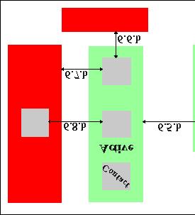
9 Design Rules consider transistors Drain Drain Layer Map Gate Gate Bulk Source Source Bulk connection needed Single bulk connection can often be used for several (many) transistors is they share the same well
10 Design Rules (example) Logic Circuit Circuit Schematic (Including Device Sizing) Stick Diagram
11 Design Rules (example) Layer Map Layout
12 Design Rules (example) Polygons merged in Geometric Description File (GDF) Separate rectangles generally more convenient to represent
13 Design Rules (example) Design rules must be satisfied throughout the design DRC runs incrementally during layout in most existing tools to flag most problems DRC can catch layout errors but not circuit design errors
14 Design Rules (example) What is wrong with this layout? Bulk connections missing!
15 Design Rules (example) Note diffusions needed for bulk connections Note p-well connections increase area a significant amount Note p-wells are both connected to V DD in this circuit
16 Design Rules (example) Layout with shared p-well reduces area
17 Design Rules (example) Shared p-active can be combined to reduce area Shared n-active can be combined to reduce area
18 Design Rules Design rules can be given in absolute dimensions for every rule Design rules can be parameterized and given relative to a parameter Makes movement from one process to another more convenient Easier for designer to remember Some penalty in area efficiency Often termed λ-based design rules Typically λ is ½ the minimum feature size in a process
19 Design Rules See for design rules
20
21
22 Design Rules See for design rules Some of these files are on class WEB site SCMOS Rules Updated Sept 2005.pdf Mosis Rules Pictorial.pdf
23 SCMOS Layout Rules - Well Page 1 of 1 SCMOS Layout Rules - Well Rule Description Lambda SCMOS SUBM DEEP 1.1 Minimum width Minimum spacing between wells at different potential Minimum spacing between wells at same potential Minimum spacing between wells of different type (if both are drawn) /13/2004
 is illustrated under Select Layout Rules.")
24 MOSIS SCMOS - Active Page 1 of 1 SCMOS Layout Rules - Active Rule Description Lambda SCMOS SUBM DEEP 2.1 Minimum width 3 * 3 * Minimum spacing Source/drain active to well edge Substrate/well contact active to well edge Minimum spacing between non-abutting active of different implant. Abutting active ("split-active") is illustrated under Select Layout Rules * Note: For analog and critical digital designs, MOSIS recommends the following minimum MOS channel widths (active under poly) for AMIS designs. Narrower devices, down to design rule minimum, will be functional, but their electrical characteristics will not scale, and their performance is not predictable from MOSIS SPICE parameters. Process Design Technology Design Lambda (micrometers) Minimum Width (lambda) AMI_ABN SCNA, SCNE AMI_C5F/N SCN3M, SCN3ME AMI_C5F/N SCN3M_SUBM, SCN3ME_SUBM /13/2004

25 MOSIS SCMOS - Poly Page 1 of 1 SCMOS Layout Rules - Poly Rule Description Lambda SCMOS SUBM DEEP 3.1 Minimum width Minimum spacing over field a Minimum spacing over active Minimum gate extension of active Minimum active extension of poly Minimum field poly to active /13/2004

26 MOSIS SCMOS - Select Page 1 of 1 SCMOS Layout Rules - Select Rule 4.1 Description Minimum select spacing to channel of transistor to ensure adequate source/drain width Lambda SCMOS SUBM DEEP Minimum select overlap of active Minimum select overlap of contact Minimum select width and spacing (Note: P-select and N-select may be coincident, but must not overlap) (not illustrated) /13/2004
, it is required that all features on the insulator layers (CONTACT, VIA, VIA2) must be of the single standard size; there are no exceptions")

27 MOSIS SCMOS - Contact Page 1 of 3 SCMOS Layout Rules - Contact to Poly On 0.50 micron process (and all finer feature size processes), it is required that all features on the insulator layers (CONTACT, VIA, VIA2) must be of the single standard size; there are no exceptions for pads (or logos, or anything else); large openings must be replaced by an array of standard sized openings. Contacts must be drawn orthogonal to the grid of the layout. Non-Manhattan contacts are not allowed. If your design cannot tolerate 1.5 lambda contact overlap in 5.2, use the alternative rules which reduce the overlap but increase the spacing to surrounding features. Rules 5.1, 5.3, and 5.4, still apply and are unchanged. Simple Contact to Poly Alternative Contact to Poly Rule Description Lambda SCMOS SUBM DEEP Rule Description SCMOS Lambda SUBM DEEP 5.1 Exact contact size 2x2 2x2 2x Minimum poly overlap Minimum contact spacing Minimum spacing to gate of transistor b 5.5.b 5.6.b 5.7.b Minimum poly overlap Minimum spacing to other poly Minimum spacing to active (one contact) Minimum spacing to active (many contacts) /13/2004
28 MOSIS SCMOS - Contact Page 2 of 3 Simple Poly to Contact Alternative C SCMOS Layout Rules - Contact to Active If your design cannot handle the 1.5 lambda contact overlap in 6.2, use the alternative rules which reduce the overlap but increase the spacing to surrounding features. Rules 6.1, 6.3, and 6.4, still apply and are unchanged. Contacts must be drawn orthogonal to the grid of the layout. Non-Manhattan contacts are not allowed. Simple Contact to Active Alternative Contact to Active Rule Description Lambda SCMOS SUBM DEEP Rule Description Lambda SCMOS SUBM DEEP 6.1 Exact contact size 2x2 2x2 2x2 6.2.b Minimum active overlap Minimum active overlap Minimum contact spacing Minimum spacing to gate of transistor b 6.6.b 6.7.b Minimum spacing to diffusion active Minimum spacing to field poly (one contact) Minimum spacing to field poly (many contacts) b Minimum spacing to poly contact /13/2004

29 MOSIS SCMOS - Contact Page 3 of 3 Simple Contact to Active Alternative Contac 9/13/2004

30 MOSIS SCMOS - Metal1 Page 1 of 1 SCMOS Layout Rules - Metal1 Rule Description Lambda SCMOS SUBM DEEP 7.1 Minimum width Minimum spacing Minimum overlap of any contact Minimum spacing when either metal line is wider than 10 lambda /13/2004

31 MOSIS SCMOS - Via, Metal2 Page 1 of 2 SCMOS Layout Rules - Via Vias must be drawn orthogonal to the grid of the layout. Non-Manhattan vias are not allowed. Lambda Rule Description 2 Metal Process 3+ Metal Process SCMOS SUBM DEEP SCMOS SUBM DEEP 8.1 Exact size 2 x 2 n/a n/a 2 x 2 2 x 2 3 x Minimum via1 spacing 3 n/a n/a Minimum overlap by metal1 1 n/a n/a Minimum spacing to contact for technology codes mapped to processes that do not allow stacked vias (SCNA, SCNE, SCN3M, SCN3MLC) 2 n/a n/a 2 2 n/a 8.5 Minimum spacing to poly or active edge for technology codes mapped to processes that do not allow stacked vias (NOTE: list is not same as for 8.4) 2 n/a n/a 2 2 n/a SCMOS Layout Rules - Metal2 Rule Description Lambda 2 Metal Process 3+ Metal Process SCMOS SUBM DEEP SCMOS SUBM DEEP 9.1 Minimum width 3 n/a n/a Minimum spacing 3 n/a n/a /13/2004

32 MOSIS SCMOS - Via, Metal2 Page 2 of Minimum overlap of via1 1 n/a n/a Minimum spacing when either metal line is wider than 10 lambda 6 n/a n/a /13/2004

33 MOSIS SCMOS - Glass Page 1 of 1 SCMOS Layout Rules - Overglass Note that rules in this section are in units of microns. They are not "true" design rules, but they do make good practice rules. Unfortunately, there are no really good generic pad design rules since pads are process-specific. Rule Description Microns 10.1 Minimum bonding passivation opening Minimum probe passivation opening Pad metal overlap of passivation Minimum pad spacing to unrelated metal Minimum pad spacing to active, poly or poly /13/2004

34 MOSIS SCMOS - Poly2 Page 1 of 3 SCMOS Layout Rules - Poly2 for Capacitor The poly2 layer is a second polysilicon layer (physically above the standard, or first, poly layer). The oxide between the two polys is the capacitor dielectric. The capacitor area is the area of coincident poly and electrode. Rule Description Lambda SCMOS SUBM DEEP 11.1 Minimum width 3 7 n/a 11.2 Minimum spacing 3 3 n/a 11.3 Minimum poly overlap 2 5 n/a 11.4 Minimum spacing to active or well edge (not illustrated) 2 2 n/a 11.5 Minimum spacing to poly contact 3 6 n/a 11.6 Minimum spacing to unrelated metal 2 2 n/a SCMOS Layout Rules - Poly2 for Transistor Same poly2 layer as for caps Rule Description Lambda SCMOS SUBM DEEP 12.1 Minimum width 2 2 n/a 12.2 Minimum spacing 3 3 n/a 12.3 Minimum electrode gate overlap of active 2 2 n/a 9/13/2004

35 MOSIS SCMOS - Poly2 Page 2 of Minimum spacing to active 1 1 n/a 12.5 Minimum spacing or overlap of poly 2 2 n/a 12.6 Minimum spacing to poly or active contact 3 3 n/a SCMOS Layout Rules - Poly2 Contact The poly2 is contacted through the standard contact layer, similar to the first poly. The overlap numbers are larger, however. Contacts must be drawn orthogonal to the grid of the layout. Non-Manhattan contacts are not allowed. Rule Description Lambda SCMOS SUBM DEEP 13.1 Exact contact size 2 x 2 2 x 2 n/a 13.2 Minimum contact spacing 2 3 n/a 13.3 Minimum electrode overlap (on capacitor) 3 3 n/a 13.4 Minimum electrode overlap (not on capacitor) 2 2 n/a 13.5 Minimum spacing to poly or active 3 3 n/a 9/13/2004

36 MOSIS SCMOS - Poly2 Page 3 of 3 9/13/2004
37 Note: Only Rules 1 through 11 are applicable to the AMI 0.5u process

38 MOSIS SCMOS - Via2, Metal3 Page 1 of 2 SCMOS Layout Rules - Via2 Vias must be drawn orthogonal to the grid of the layout. Non-Manhattan vias are not allowed. Lambda Rule Description 3 Metal Process 4+ Metal Process SCMOS SUBM DEEP SCMOS SUBM DEEP 14.1 Exact size 2x2 2x2 n/a 2x2 2x2 3x Minimum spacing 3 3 n/a Minimum overlap by metal2 1 1 n/a Minimum spacing to via1 for technology codes that do not allow stacked vias (SCNA, SCNE, SCN3M, SCN3ME, SCN3MLC) 2 2 n/a 2 2 n/a 14.5 Via2 may be placed over contact SCMOS Layout Rules - Metal3 9/13/2004

39 MOSIS SCMOS - Via2, Metal3 Page 2 of 2 Rule Description Lambda 3 Metal Process 4+ Metal Process SCMOS SUBM DEEP SCMOS SUBM DEEP 15.1 Minimum width 6 5 n/a Minimum spacing to metal3 4 3 n/a Minimum overlap of via2 2 2 n/a Minimum spacing when either metal line is wider than 10 lambda 8 6 n/a /13/2004
40 MOSIS SCMOS - PBASE Page 1 of 2 SCMOS Layout Rules - Pbase (Analog Option) The pbase layer is an active area that is implanted with the pbase implant to form the base of the NPN bipolar transistor. The base contact is enclosed in p-select. The emitter is an n-select region within (and on top of) the base. The entire pbase sits in an n-well that is the collector. The collector contact is a well contact, but the overlaps are larger. Active should not be used inside of pbase. Rule Description Lambda SCMOS SUBM DEEP 16.1 All active contact 2 x 2 n/a n/a 16.2 Minimum emitter select overlap of contact 3 n/a n/a 16.3 Minimum pbase overlap of emitter select 2 n/a n/a 16.4 Minimum spacing between emitter select and base select 4 n/a n/a 16.5 Minimum pbase overlap of base select 2 n/a n/a 16.6 Minimum base select overlap of contact 2 n/a n/a 16.7 Minimum nwell overlap of pbase 6 n/a n/a 16.8 Minimum spacing between pbase and collector active 4 n/a n/a 16.9 Minimum collector active overlap of contact 2 n/a n/a Minimum nwell overlap of collector active 3 n/a n/a Minimum select overlap of collector active 2 n/a n/a 9/13/2004

41 MOSIS SCMOS - PBASE Page 2 of 2 9/13/2004
42 MOSIS SCMOS - Capacitor Well Page 1 of 2 SCMOS Layout Rules - Capacitor Well The capacitor well described in this and the next rule only apply to SCN3MLC and SCN3MLC_SUBM technology codes manufactured on an Agilent/HP AMOS14TB run. Rule Description Lambda SCMOS SUBM DEEP 17.1 Minimum width n/a 17.2 Minimum spacing 9 18 n/a 17.3 Minimum spacing to external active 5 6 n/a 17.4 Minimum overlap of active 5 6 n/a SCMOS Layout Rules - Linear Capacitor (Linear Capacitor Option) These rules illustrate the construction of a linear capacitor in a capacitor well. The capacitor itself is the region of overlapped poly and active. The active area is electrically connected to the cap well Rule Description Lambda SCMOS SUBM DEEP 18.1 Minimum width 3 3 n/a 18.2 Minimum poly extension of active 2 2 n/a 18.3 Minimum active overlap of poly 3 3 n/a 18.4 Minimum poly contact to active 2 2 n/a 18.5 Minimum active contact to poly 6 6 n/a 9/13/2004

43 MOSIS SCMOS - Capacitor Well Page 2 of 2 9/13/2004
44 MOSIS SCMOS - Silicide Block Page 1 of 2 SCMOS Layout Rules - Silicide Block Rule Description Lambda SCMOS SUBM DEEP 20.1 Minimum SB width Minimum SB spacing Minimum spacing, SB to contact (no contacts allowed inside SB) Minimum spacing, SB to external active Minimum spacing, SB to external poly Resistor is poly inside SB; poly ends stick out for contacts the entire resistor must be outside well and over field 20.7 Minimum poly width in resistor Minimum spacing of poly resistors (in a single SB region) Minimum SB overlap of poly or active Minimum poly or active overlap of SB Minimum spacing, SB to poly (in a single active region) NOTE: Some processes do not support both silicide block over active and silicide block over poly. Refer to the individual process description pages. 9/13/2004

45 MOSIS SCMOS - Silicide Block Page 2 of 2 9/13/2004

46 MOSIS SCMOS - Metal4 Page 1 of 2 SCMOS Layout Rules - Via3 Vias must be drawn orthogonal to the grid of the layout. Non-Manhattan vias are not allowed. Lambda Rule Description 4 metal Process 5+ Metal Process SCMOS SUBM DEEP SCMOS SUBM DEEP 21.1 Exact size 2x2 2x2 n/a n/a 2x2 3x Minimum spacing 3 3 * n/a n/a Minimum overlap by Metal3 1 1 n/a n/a 1 1 * Exception: Use lambda=4 for rule 21.2 only when using SCN4M_SUBM for Agilent/HP GMOS10QA 0.35 micron process SCMOS Layout Rules - Metal4 9/13/2004

47 MOSIS SCMOS - Metal4 Page 2 of 2 Rule Description Lambda 4 Metal Process 5+ Metal Process SCMOS SUBM DEEP SCMOS SUBM DEEP 22.1 METAL4 width 6 6 n/a n/a METAL4 space 6 6 n/a n/a METAL4 overlap of VIA3 2 2 n/a n/a Minimum spacing when either metal line is wider than 10 lambda n/a n/a /13/2004
48 MOSIS SCMOS - PolyCap Page 1 of 2 SCMOS Layout Rules - SCNPC with POLY_CAP The two plates of an SCNPC capacitor are POLY and POLY_CAP1. The POLY_CAP1 must surround the POLY everywhere; the area of the capacitor is the area of the POLY. POLY is physically on top of POLY_CAP1, so that contact to the POLY_CAP1 must be made in the region where it extends beyond the POLY. The capacitor may be in the well or the substrate, but may not straddle a well boundary. The only metal that may cross over a capacitor is the connecting METAL1 wires. Rule Description Minimum POLY_CAP1 width. This is lithographic; the minimum to build a real capacitor is greater than 12 lambda Minimum spacing, POLY_CAP1 to POLY_CAP1 (neighboring capacitor) Minimum spacing, POLY_CAP1 to ACTIVE (all capacitors must be over field) Lambda SCMOS SUBM DEEP 8 n/a n/a 4 n/a n/a 8 n/a n/a 23.4 Minimum overlap, POLY_CAP1 over POLY 3 n/a n/a 23.5 Minimum overlap, POLY_CAP1 over CONTACT 2 n/a n/a 23.6 Minimum overlap, POLY over CONTACT (in a capacitor only; still 1 lambda elsewhere) 2 n/a n/a 23.7 Minimum spacing, POLY to CONTACT-to-POLY_CAP1 2 n/a n/a 23.8 Minimum spacing, unrelated METAL1 to POLY_CAP1 4 n/a n/a 23.9 Minimum spacing, METAL2 to POLY_CAP1 2 n/a n/a 9/13/2004

49 MOSIS SCMOS - PolyCap Page 2 of 2 9/13/2004
50 MOSIS SCMOS - Thick Active Page 1 of 1 SCMOS Layout Rules - Thick Active THICK_ACTIVE is a layer used for those processes offering two different thicknesses of gate oxide (typically for the layout of transistors that operate at two different voltage levels). The ACTIVE layer is used to delineate all the active areas, regardless of gate oxide thickness. THICK_ACTIVE is used to mark those ACTIVE areas that will have the thicker gate oxide; ACTIVE areas outside THICK_ACTIVE will have the thinner gate oxide. THICK_ACTIVE by itself (not covering any ACTIVE polygon) is meaningless. Rule Description Lambda SCMOS SUBM DEEP 24.1 Minimum width Minimum spacing Minimum ACTIVE overlap Minimum space to external ACTIVE Minimum poly width in a THICK_ACTIVE gate Every ACTIVE region is either entirely inside THICK_ACTIVE or entirely outside THICK_ACTIVE 9/13/2004
51 MOSIS SCMOS - Metal5 Page 1 of 1 SCMOS Layout Rules - Via4 (SUBM and DEEP) Vias must be drawn orthogonal to the grid of the layout. Non-Manhattan vias are not allowed. Lambda Rule Description 5 Metal Process 6+ Metal Process SCMOS SUBM DEEP SCMOS SUBM DEEP 25.1 Exact size n/a 2x2 3x3 n/a 2x2 3x Minimum spacing n/a 3 3 n/a Minimum overlap by Metal4 n/a 1 1 n/a 1 1 SCMOS Layout Rules - Metal5 (SUBM and DEEP) Any designer using the SCMOS rules who wants the TSMC Thick_Top_Metal must draw the top metal to comply with the TSMC rules for that layer. Lambda Rule Description 5 Metal Process 6+ Metal Process SCMOS SUBM DEEP SCMOS SUBM DEEP 26.1 Minimum width n/a 4 4 n/a Minimum spacing to Metal5 n/a 4 4 n/a Minimum overlap of Via4 n/a 1 2 n/a Minimum spacing when either metal line is wider than 10 lambda n/a 8 8 n/a /13/2004
52 MOSIS SCMOS - High Res Page 1 of 1 SCMOS Layout Rules - High Res Rule Description Lambda SCMOS SUBM DEEP 27.1 Minimum HR width 4 4 n/a 27.2 Minimum HR spacing 4 4 n/a 27.3 Minimum spacing, HR to contact (no contacts allowed inside HR) 2 2 n/a 27.4 Minimum spacing, HR to external active 2 2 n/a 27.5 Minimum spacing, HR to external poly2 2 2 n/a 27.6 Resistor is poly2 inside HR; poly2 ends stick out for contacts, the entire resistor must be outside well and over field 27.7 Minimum poly2 width in resistor 5 5 n/a 27.8 Minimum spacing of poly2 resistors (in a single HR region) 7 7 n/a 27.9 Minimum HR overlap of poly2 2 2 n/a 9/13/2004
53 MOSIS SCMOS - CAP_TOP_METAL Page 1 of 2 SCMOS Layout Rules - CAP_TOP_METAL for SCMOS_DEEP (and SUBM) The CAP_TOP_METAL layer is used exclusively for the construction of metal-to-metal capacitors. The bottom plate of the capacitor is one of the regular metal layers, as specified below. CAP_TOP_METAL is the upper plate of the capacitor; it is sandwiched physically between the bottom plate metal and the next metal layer above, with a thin dielectric between the bottom plate and the upper (CAP_TOP_METAL) plate. The CAP_TOP_METAL can only be contacted from the metal above; the bottom plate metal can be contacted from below or above (subject, in either case, to rule 28.5), and/or by bottom metal extending outside of the capacitor region (rule 28.7). Use of all (legal) upward vias within that region should be maximized. CAP_TOP_METAL must always be contained entirely within the bottom plate metal. Process Bottom Plate Top Plate Top Plate Contact TSMC_025 METAL4 CAP_TOP_METAL VIA4 and METAL5 TSMC_018 METAL5 CAP_TOP_METAL VIA5 and METAL6 Rule Description Lambda SCMOS SUBM DEEP 28.1 Minimum Width, Capacitor n/a Minimum Spacing (2 capacitors sharing a single bottom plate) Minimum bottom metal overlap (including dummy shapes) n/a n/a Minimum overlap of via n/a Minimum spacing to bottom metal via n/a Minimum bottom metal overlap of its via n/a Rule applicability region extends beyond bottom plate n/a Minimum width, dummy shapes (having no vias) n/a Minimum bottom plate to other bottom plate metal n/a Minimum via separation, on CAP_TOP_METAL n/a Minimum (upward) via separation on bottom metal n/a Maximum CAP_TOP_METAL width and length n/a 30 um Maximum bottom metal plate width and length n/a 35 um 9/13/2004
54 MOSIS SCMOS - CAP_TOP_METAL Page 2 of No vias from bottom plate downward, directly under top plate CAP_TOP_METAL; dummy metal shapes under capacitor region, discouraged No active or passive circuitry under capacitor region 9/13/2004
55 MOSIS SCMOS - Metal6 Page 1 of 1 SCMOS Layout Rules - Via5 (SUBM and DEEP) Vias must be drawn orthogonal to the grid of the layout. Non-Manhattan vias are not allowed. Lambda Rule Description 6 Metal Process SCMOS SUBM DEEP 29.1 Exact size n/a 3 x 3 4 x Minimum spacing n/a Minimum overlap by Metal5 n/a 1 1 SCMOS Layout Rules - Metal6 (SUBM and DEEP) Any designer using the SCMOS rules who wants the TSMC Thick_Top_Metal must draw the top metal to comply with the TSMC rules for that layer. Lambda Rule Description 6 Metal Process SCMOS SUBM DEEP 30.1 Minimum width n/a Minimum spacing to Metal6 n/a Minimum overlap of Via5 n/a Minimum spacing when either metal line is wider than 10 lambda n/a /13/2004
56 MOSIS SCMOS - DEEP_N_WELL Page 1 of 2 SCMOS Layout Rules - DEEP_N_WELL for SCMOS_DEEP (and SUBM) The DEEP_N_WELL layer provides access to the DNW layer in the TSMC 0.18 and 0.25 processes. This provides a layering sometimes called "triple-well" in which an n-well sits in the p-substrate, and then a p-well sits fully inside of the n-well; it is then possible to construct NMOS devices inside of that isolated p-well. The isolated p-well is surrounded by a fence of standard N_WELL (around its periphery), and by DEEP_N_WELL underneath. The N_WELL fence makes direct electrical contact with the DEEP_N_WELL plate beneath it. DEEP_N_WELL is available in technology codes SCN5M_SUBM, SCN5M_DEEP, SCN6M_SUBM and SCN6M_DEEP but only where these are to be fabricated on TSMC foundry runs. To gain a better understanding of this layer, the TSMC vendor-rule design rule documentation should be studied. Rule Description Lambda SCMOS SUBM DEEP 31.1 Minimum Width, Deep_N_Well n/a Minimum Spacing, Deep_N_Well to Deep_N_Well n/a Minimum extension, N_Well beyond Deep_N_Well edge n/a Minimum overlap, N_Well over Deep_N_Well edge n/a Minimum spacing, Deep_N_Well to unrelated N_Well n/a Minimum spacing, N+Active in isolated P-well, to N_Well n/a Minimum spacing, external N+Active to Deep_N_Well n/a Minimum spacing, P+Active in N_Well to its Deep_N_Well n/a /13/2004

57 MOSIS SCMOS - DEEP_N_WELL Page 2 of 2 9/13/2004
58 IC Fabrication Technology See Chapter 1 and 3 of WH or Chapter 2 GAS for details
59 IC Fabrication Technology Crystal Preparation Masking Photolithographic Process Deposition Etching Diffusion Oxidation Epitaxy Polysilicon Contacts, Interconnect and Metalization Planarization
60 Generic Process Flow Front End W afer Fabrication Mask Fabrication Epitaxy Grow or Apply Photoresist Deposit or Implant Etch Strip Planarization Wafer Probe Back End Wafer Dicing Die Attach W ire Attach (bonding) Package Test Ship
61 Review MOS Transistor A A Drain Gate Bulk Source Gate Drain Source n-channel MOSFET
62 Review MOS Transistor A A Drain Gate Source Gate Drain Source Bulk p-channel MOSFET
63 n-channel MOS transistor in Bulk CMOS n-well process with bulk contact MOS Transistor
64 p-channel MOS transistor in Bulk CMOS n-well process with bulk contact and well (tub) MOS Transistor
65 Crystal Preparation Large crystal is grown (pulled) 12 inches in diameter and 1 to 2 m long Sliced to 250u to 500u thick Prefer to be much thinner but thickness needed for mechanical integrity 4 to 8 cm/hr pull rate T=1430 o C Crystal is sliced to form wafers Cost for 12 wafer around $200 5 companies provide 90% of worlds wafers Somewhere around 400,000 12in wafers/month
66 Crystal Preparation 12in 1 to 2 m 250u tp 500u Lightly-doped silicon Excellent crystalline structure
67 Crystal Preparation From

68 Crystal Preparation Source: WEB

69 Crystal Preparation Source: WEB

70 Crystal Preparation Source: WEB

71 Crystal Preparation Source: WEB

72 Crystal Preparation Source: WEB
MOSIS LAMBDA DESIGN RULES
 MOSIS LAMBDA DESIGN RULES 3 sets of design rules: 1) SCMOS: valid for technologies with 2λ>1 µm 2) SCMOS_SUBM: valid for technologies with 0.25
VLSI Design I; A. Milenkovic 1
 Switch Model of NMOS Transistor V GS Gate CPE/EE 47, CPE 57 VLSI Design I L0: IC Manufacturing Source (of carriers) Drain (of carriers) Department of Electrical and Computer Engineering University of Alabama
CPE/EE 427, CPE 527 VLSI Design I IC Manufacturing. The MOS Transistor
 CPE/EE 427, CPE 527 VLSI Design I IC Manufacturing Department of Electrical and Computer Engineering University of Alabama in Huntsville Aleksandar Milenkovic The MOS Transistor Polysilicon Aluminum 9/11/2006
THIẾT KẾ VI MẠCH TƯƠNG TỰ CHƯƠNG 2: CMOS Technology
 THIẾT KẾ VI MẠCH TƯƠNG TỰ CHƯƠNG 2: CMOS Technology Hoàng Trang-bộ môn Kỹ Thuật Điện Tử hoangtrang@hcmut.edu.vn 1 TP.Hồ Chí Minh 12/2011 1. Overview - IC technology - CMOS vs BJT Hoàng Trang-bộ môn Kỹ
ECE520 VLSI Design. Lecture 9: Design Rules. Payman Zarkesh-Ha
 ECE520 VLSI Design Lecture 9: Design Rules Payman Zarkesh-Ha Office: ECE Bldg. 230B Office hours: Wednesday 2:00-3:00PM or by appointment E-mail: pzarkesh@unm.edu Slide: 1 Review of Last Lecture Interconnect
Philips SAA7118E Multi Standard Video Decoder Process Review
 March 31, 2006 Philips SAA7118E Multi Standard Video Decoder Process Review For comments, questions, or more information about this report, or for any additional technical needs concerning semiconductor
Layout Design II. Lecture Fall 2003
 Layout Design II Lecture 6 18-322 Fall 2003 Roadmap Today: Layout Verification & design in the large Next week: Transistor sizing Wires Homework 1: Due Today Homework 2: Out Today, Due Sept 18 Lab 2: This
Design and Technology Solutions for Development of SiGeMEMS devices. Tom Flynn Vice President, Sales Coventor
 Design and Technology Solutions for Development of SiGeMEMS devices Tom Flynn Vice President, Sales Coventor Special thanks to: Stephane Donnay, Program Manager, imec Gerold Schropfer, Director, Foundary
Freescale Semiconductor MMA6222AEG ±20/20g Dual-Axis Medium-g Micromachined HARMEMS Accelerometer
 Freescale Semiconductor MMA6222AEG ±20/20g Dual-Axis Medium-g Micromachined HARMEMS Accelerometer MEMS Process Review For comments, questions, or more information about this report, or for any additional
STMicroelectronics LISY300AL Single-Axis Analog Yaw Rate Gyroscope
 Single-Axis Analog Yaw Rate Gyroscope MEMS Process Review For comments, questions, or more information about this report, or for any additional technical needs concerning semiconductor technology, please
Physical Design of CMOS Integrated Circuits
 Physical Design of CMOS Integrated Circuits Dae Hyun Kim EECS Washington State University References John P. Uyemura, Introduction to VLSI Circuits and Systems, 2002. Chapter 5 Goal Understand how to physically
Glass Frit Wafer Bonding Sealed Cavity Pressure in Relation to Bonding Process Parameters. Roy Knechtel, Sophia Dempwolf, Holger Klingner
 10.1149/07509.0255ecst The Electrochemical Society Glass Frit Wafer Bonding Sealed Cavity Pressure in Relation to Bonding Process Parameters Roy Knechtel, Sophia Dempwolf, Holger Klingner X-FAB MEMS Foundry
Long term stability tests of INO RPC prototypes
 Long term stability tests of INO RPC prototypes While the problem of sudden aging in the glass RPC prototypes is being investigated, a few RPCs of dimension 40 cm 30 cm were fabricated, using glass procured
TOTAL-IONIZING-DOSE RESPONSE OF 65 nm MOSFETS IRRADIATED TO ULTRA- HIGH DOSES. GIULIO BORGHELLO
 TOTAL-IONIZING-DOSE RESPONSE OF 65 nm MOSFETS IRRADIATED TO ULTRA- HIGH DOSES GIULIO BORGHELLO giulio.borghello@cern.ch introduction Presented at NSREC 2017 14/11/2017 GIULIO BORGHELLO 2 introduction Presented
VLSI Design 12. Design Styles
 1 9 8 5 1 9 8 7 1 9 9 1 1 9 9 3 1 9 9 9 2 0 0 1 2 0 0 5 2 0 0 7 2 0 0 9 Pr odu ctiv it y (T r an s./ St a f -M o nt h ) VLSI Design Last module: Floorplanning Sequential circuit design Clock skew This
DESIGN AND CHARACTERIZATION OF 20NM SOI MOSFET DOPING ABRUPTNESS DEPENDENT
 DESIGN AND CHARACTERIZATION OF 20NM SOI MOSFET DOPING ABRUPTNESS DEPENDENT A. S. M. Zain 1, N. F. M. Zain 2, F. Salehuddin 1, N. Jamaluddin 2 and N. Abdullah Yaacob 2 1 Centre for Telecommunication Research
TEPZZ A_T EP A1 (19) (11) EP A1 (12) EUROPEAN PATENT APPLICATION. (51) Int Cl.: G01L 9/00 ( )
 (11) EP A1 (12) EUROPEAN PATENT APPLICATION. (51) Int Cl.: G01L 9/00 ( )") (19) TEPZZ 796844A_T (11) EP 2 796 844 A1 (12) EUROPEAN PATENT APPLICATION (43) Date of publication: 29..2014 Bulletin 2014/44 (51) Int Cl.: G01L 9/00 (2006.01) (21) Application number: 13165416.2 (22)
(19) TEPZZ 796844A_T (11) EP 2 796 844 A1 (12) EUROPEAN PATENT APPLICATION (43) Date of publication: 29..2014 Bulletin 2014/44 (51) Int Cl.: G01L 9/00 (2006.01) (21) Application number: 13165416.2 (22)
CPE/EE 427, CPE 527 VLSI Design I L06: Complementary CMOS Logic Gates
 PE/EE 427, PE 527 VLSI esign I L6: omplementary MOS Logic Gates epartment of Electrical and omputer Engineering University of labama in Huntsville leksandar Milenkovic ( www.ece.uah.edu/~milenka ) www.ece.uah.edu/~milenka/cpe527-5f
Random Diffusion Masking Defect
 Random Diffusion Masking Defect By Christopher Henderson In this article we will discuss a failure mechanism that has been around for as long as the semiconductor lithography process the mask defect. To
VLSI Design 14. Memories
 Last module: Synthesis and Verilog This module Memory arrays SRMs Serial Memories Dynamic memories Memory rrays Memory rrays Random ccess Memory Serial ccess Memory Content ddressable Memory (CM) Read/Write
Errata CMOS VLSI Design 3 rd Edition
 Errata CMOS VLSI esign 3 rd Edition Last updated 4 September 2006 Send your corrections to bugs@cmosvlsi.com Errata in 2 nd Printing Page viii, Section 4.3: SIzing -> Sizing (N. Ho 8/16/06) Page 39, Table
Pressure Sensor Bridge Configurations
 Pressure Sensor Bridge Configurations 1. Purpose Describe different pressure sensor bridge configurations, when each can and cannot be used, and the advantages and disadvantages of each. 2. Introduction
21 rue La Nouë Bras de Fer Nantes - France Phone : +33 (0) website :
 website :") 21 rue La Nouë Bras de Fer - 44200 Nantes - France Phone : +33 (0) 240 180 916 - email : info@systemplus.fr - website : www.systemplus.fr April 2013 - Version 1 Written by: Romain FRAUX DISCLAIMER : System
21 rue La Nouë Bras de Fer - 44200 Nantes - France Phone : +33 (0) 240 180 916 - email : info@systemplus.fr - website : www.systemplus.fr April 2013 - Version 1 Written by: Romain FRAUX DISCLAIMER : System
Section 2 WHAT DO THE BULBS DO TO MOVING CHARGE?
 Section 2 WHAT DO THE BULBS DO TO MOVING CHARGE? INTRODUCTION We know the filaments of bulbs connected to batteries give off heat and light. We will now investigate how bulb filaments also control the
EE241 - Spring 2013 Advanced Digital Integrated Circuits. Assigned reading. No new reading. Lecture 4: Transistor Models
 EE41 - Spring 013 Advanced Digital Integrated ircuits ecture 4: Transistor Models Assigned reading No new reading 1 Outline ast lecture Features of modern technologies This lecture Transistor modeling
Manufacturing Processes for WSi 2 -GPSOI Substrates and their Influence on Cross-talk Suppression and Inductance
 Manufacturing Processes for WSi 2 -GPSOI Substrates and their Influence on Cross-talk Suppression and Inductance PT Baine*, HS Gamble *, BM Armstrong *, DW McNeill *, M Bain* J Hamel #, S Stefanos +, M
TEPZZ 6 7ZZ7A_T EP A1 (19) (11) EP A1 (12) EUROPEAN PATENT APPLICATION. (51) Int Cl.: G01L 9/00 ( ) G01L 27/00 (2006.
 (11) EP A1 (12) EUROPEAN PATENT APPLICATION. (51) Int Cl.: G01L 9/00 ( ) G01L 27/00 (2006.") (19) TEPZZ 6 7ZZ7A_T (11) EP 2 637 007 A1 (12) EUROPEAN PATENT APPLICATION (43) Date of publication: 11.09.13 Bulletin 13/37 (1) Int Cl.: G01L 9/00 (06.01) G01L 27/00 (06.01) (21) Application number: 1218617.6
(19) TEPZZ 6 7ZZ7A_T (11) EP 2 637 007 A1 (12) EUROPEAN PATENT APPLICATION (43) Date of publication: 11.09.13 Bulletin 13/37 (1) Int Cl.: G01L 9/00 (06.01) G01L 27/00 (06.01) (21) Application number: 1218617.6
DIY - PC - Interface for Suunto Cobra/Vyper/Mosquito
 DIY - PC - Interface for Suunto Cobra/Vyper/Mosquito Summary This document is the distinct consequence of the Spyder/Stinger interface DIY. After having many e-mails concerning the application for the
EE 432 Lab 3 PMOS source/drain lithography and diffusion
 EE 432 Lab 3 PMOS source/drain lithography and diffusion Group Leader: Yue Zhang Group Numbers: Yueyi Jiao, Yin Huang, Lafit Masud TA: Andy Hoyt Section: NO. 5 Introduction: In this lab, we will perform
ProChek, A COMPREHENSIVE FABRICATION PROCESS MISMATCH AND RELIABILITY CHARACTERIZATION TOOL
 Vendor: Ridgetop Group, Inc. Office Address: 3580 West Ina Road, Tucson, Arizona 85741 Phone: 520-742-3300; Fax: 520-544-3180 Technical Contact: Esko Mikkola, Ph.D., Project Manager Phone: 520-742-3300
CD4008BMS. CMOS 4-Bit Full Adder With Parallel Carry Out. Features. Pinout. Logic Diagram. Applications. Description.
 CD48BMS November 994 CMOS 4-Bit Full Adder With Parallel Carry Out Features Pinout High-Voltage Type (2V Rating) 4 Sum Outputs Plus Parallel Look-ahead Carry-Output CD48BMS TOP VIEW High-Speed Operation
Guidelines to the standard IEC60601
 EUROPEAN POWER SUPPLY MANUFACTURERS ASSOCIATION (Visit the EPSMA website at www.epsma.org) Medical Approvals for Power Supplies Guidelines to the standard IEC60601 Revision Date: 2009-09-12 This document
CrimpFlex Crimping Guidelines
 The following guidelines are suggestions to the design engineer and quality control personnel on proven methods of incorporating the CrimpFlex? contact into their designs and into their manufacturing and
Technical Data Sheet MF010-O-LC
 Technical Data Sheet MF010-O-LC - 1 - 1. Properties The oxygen measuring system MF010-O-LC determines the oxygen content in gas mixtures up to a temperature of 250 C. It is particularly suitable for the
Preliminary Datasheet
 Device Features Low Noise Figure: NF = 0.95 @ 1900MHz High Linearity: OIP3 = 36 dbm @ 1900 MHz Output P1 db = 22 dbm @ 1900 MHz Gain = 17 db @ 1900 MHz Internally matched to 50 ohms Vdd: 5.0V Lead-free/RoHS-compliant
Stack Height Analysis for FinFET Logic and Circuit
 2015 Spring ECE 7332 Stack Height Analysis for FinFET Logic and Circuit Xinfei Guo & Qing Qin May 8 th, 2015 Outline Background & Motivation FinFET Design and Simulation Flow Stack Height Analysis A Case
From Fundamental Detector Research to Industrial Embedded Power Device Technology Development
 From Fundamental Detector Research to Industrial Embedded Power Device Technology Development Joint Instrumentation Seminar DESY, Hamburg University and XFEL Colloquium in honor of Prof. Gunnar Lindström's
(12) United States Patent
 United States Patent") USOO9403674B2 (12) United States Patent Cheng et al. (54) METHODS FOR PACKAGING A MCROELECTROMECHANICAL SYSTEM (MEMS) WAFER AND APPLICATION-SPECIFIC INTEGRATED CIRCUIT (ASIC) DIES USING THROUGH MOLD VIAS
USOO9403674B2 (12) United States Patent Cheng et al. (54) METHODS FOR PACKAGING A MCROELECTROMECHANICAL SYSTEM (MEMS) WAFER AND APPLICATION-SPECIFIC INTEGRATED CIRCUIT (ASIC) DIES USING THROUGH MOLD VIAS
Series AM3T-VZ 3 Watt DC-DC Converter
 Click on Series name for product info on aimtec.com Series AM3T-VZ FEATURES: Wide 2:1 Range 24 Pin DIP Package High up to 82% Metal Package Operating Temperature -4 o C to +85 o C / Isolation 15 or 35
USER'S GUIDE. Digital Barometers with Analog Output PTB210 Series M210670EN-B
 USER'S GUIDE Digital Barometers with Analog Output PTB210 Series M210670EN-B PUBLISHED BY Vaisala Oyj Phone (int.): +358 9 8949 1 P.O. Box 26 Fax: +358 9 8949 2227 FIN-00421 Helsinki Finland Visit our
Type 715P/717P, Orange Drop, High Voltage, Polypropylene Film/Foil
 Type 715P/717P are high AC voltage, film/foil polypropylene capacitors. Well suited for high AC voltage applications requiring corona free performacnce. These capacitors are ideal in high frequency, high
Instrumentation & Data Acquisition Systems
 Instrumentation & Data Acquisition Systems Section 4 - Pressure Robert W. Harrison, PE Bob@TheHarrisonHouse.com Made in USA 1 Definition of Pressure Pressure is the amount of force applied perpendicular
AMS 2710 PCB pressure sensor module with V output
 FEATURES Universal pressure sensor module with 0.. 10 V voltage output Fully calibrated and temperature compensated sensor module Variants for (bidirectional) differential, gage, absolute and barometric
MANUAL KPS Pressure Control Valve
 TetraTec Instruments GmbH Gewerbestrasse 8 71144 Steinenbronn Deutschland E-Mail: info@tetratec.de Tel.: 07157/5387-0 Fax: 07157/5387-10 MANUAL Pressure Control Valve *** VERSION 1.0 *** Update: 17.11.2006
D-PAK Voiding: A Study to Determine the Origins of D-PAK Voiding
 As originally published in the SMTA Proceedings D-PAK Voiding: A Study to Determine the Origins of D-PAK Voiding Kim Flanagan and Greg Wade Indium Corporation Clinton, NY Abstract Voiding in bottom termination
Scaling. Krish Chakrabarty 1. Scaling
 Scaling Transistors Interconnect Future Challenges Krish Chakrabarty 1 Scaling The only constant in VLSI is constant change Feature size shrinks by 30% every 2-3 years Transistors become cheaper Transistors
PTB210 Series Digital Barometers with Analog Output USER'S GUIDE
 PTB210 Series Digital Barometers with Analog Output USER'S GUIDE M210670en-A December 2004 PUBLISHED BY VAISALA Oyj Phone (int.): (+358 9) 894 91 P.O. Box 26 Telefax: (+358 9) 894 9227 FIN-00421 Helsinki
Dissolved Oxygen Guide
 Educat i onser i es Di ssol vedoxygengui de Dissolved Oxygen Guide Introduction Dissolved oxygen probes provide a convenient approach to essentially direct measurement of molecular oxygen. The membrane
H Robotics Engineering Challenge
 2018 4-H Robotics Engineering Challenge The 4-H Robotics Challenge provides an opportunity for 4-H members interested in science, engineering and technology to participate in a hands on, team based activity
Lab 4 VGA Display Snake Game
 Lab 4 VGA Display Snake Game Design and implement a digital circuit capable of displaying predefined patterns on the screen of a VGA monitor, and provide the basic components for the Snake game. Your circuit
 Concurrent Design to Achieve High Performance and Low Cost: Case Study of a MEMS Automotive Pressure Sensor Design Presented by David DiPaola, Managing Director, DiPaola Consulting Moderated by Rob O'Reilly,
Thin-Film Technology. Accu-F / Accu-P Thin-Film RF/Microwave Capacitors.
 Thin-Film Technology Accu-F / Accu-P Thin-Film RF/Microwave Capacitors 5 Accu-F / Accu-P Thin-Film Technology THE IDEAL CAPACITOR The non-ideal characteristics of a real capacitor can be ignored at low
CBC2 performance with switched capacitor DC-DC converter. systems meeting, 12/2/14
 CBC2 performance with switched capacitor DC-DC converter systems meeting, 12/2/14 1 reminder of results from CBC1 +2.5V GND 1n can power CBC from single +2.5V supply 1uF DC-DC diff. clock (CMOS) 1 MHz
MS54XX Miniature SMD Pressure Sensor
 SPECIFICATIONS 1, 7, 12, and 70 bar absolute pressure range Uncompensated Piezoresistive silicon micromachined sensor Miniature surface mount Ceramic carrier Low noise, high sensitivity, high linearity
VLSI Design I; A. Milenkovic 1
 PE/EE 427, PE 527 VLI esign I L8: Pass Transistor Logic epartment of Electrical and omputer Engineering University of labama in Huntsville leksandar Milenkovic ( www. ece.uah.edu/~milenka ) www. ece.uah.edu/~milenka/cpe527-3f
CONTENTS TABLE OF MAIDA S HISTORY TERMINOLOGY & GENERAL SPECIFICATIONS. iii. LEAD CODES and TAPE & REEL STANDARD SERIES 1 HC SERIES 17
 TABLE OF CONTENTS MAIDA S HISTORY TERMINOLOGY & GENERAL LEAD CODES and TAPE & REEL i ii iii STANDARD SERIES 1 HC SERIES 17 LOW PROFILE SERIES 33 THERMALLY PROTECTED SERIES 39 HIGH ENERGY SERIES LEAD CODES
Influence of HALO and drain-extension doping gradients on transistor performance
 Materials Science and Engineering B 114 115 (2004) 15 19 Influence of HALO and drain-extension doping gradients on transistor performance Axel Erlebach a,, Thomas Feudel b, Andreas Schenk c, Christoph
Usage Policies Notebook for STS DRIE System
 Usage Policies Notebook for STS DRIE System Revision date September 2014 2 Emergency Plan for STS DRIE System Standard Operating Procedures for Emergencies Contact information Person Lab Manager Director
KNOTLESS SCREEN PRINTING FOR CRYSTALLINE SILICON SOLAR CELLS
 KNOTLESS SCREEN PRINTING FOR CRYSTALLINE SILICON SOLAR CELLS 7th Workshop on Metallization Konstanz - October 23, 2017 Y. Zhang 1, L. Zhang 2, L. Jiang 1, L. Song 1, C. Guo 1, V. Dua 1, H. Yang 1, E. Kim
A hose layline contains important information for specifying the replacement assembly: manufacturer, hose trade name, working pressure and hose ID.
 CONTENTS Introduction Pressure Pressure Drop Temperature Rating Bend Radius Conclusion Additional Information SIDEBAR: Understanding Hydraulic Hose Reinforcement INTRODUCTION Hydraulic hose has a finite
Digital electro-pneumatic regulators Series ER100
 CATALOGUE > Release 8.2 Digital electro-pneumatic regulators Series ER100 TREATMENT > Digital electro-pneumatic regulators Series ER100 Port G1/4» Compact design» Digital display» Analog and digital input»
JSP. MKT Series J S P -
 Loose Taped Fig.1 Fig. 2 JSP Typical applications: blocking, coupling, decoupling, by-passing, interference suppression in low voltage applications (i.e.:automotive) Ød ±0.05 All dimensions are in mm.
MEMS for automotive and consumer electronics
 MEMS for automotive and consumer MEMS for automotive and consumer electronics Dr. Jiri Marek Senior Vice President Engineering Sensors Robert Bosch GmbH, Automotive Electronics 1 Automotive Electronics
MIL-STD-883G METHOD
 STEADY-STATE LIFE 1. PURPOSE. The steady-state life test is performed for the purpose of demonstrating the quality or reliability of devices subjected to the specified conditions over an extended time
BAROMETER PRESSURE STANDARD PRESSURE CONTROLLER
 BAROMETER PRESSURE STANDARD PRESSURE CONTROLLER Features ±0.01% FS Measurement & Control Accuracy ±0.001% /ºC Thermal Stability Pressure Ranges from ±1 psid to 1200 psia Applications Barometric Measurement
SG33KTL-M Quick Installation Guide. 1 Unpacking and Inspection
 SG33KTL-M Quick Installation Guide This guide provides a general instruction of the installation procedures of SG33KTL-M. In no case shall this guide substitute for the user manual or related notes on
SG36KTL-M Quick Installation Guide. 1 Unpacking and Inspection
 SG36KTL-M Quick Installation Guide This guide provides a general instruction of the installation procedures of SG36KTL-M. In no case shall this guide substitute for the user manual or related notes on
The MRL Furnaces USED FOR THIS MANUAL COVERS
 The MRL Furnaces USED FOR 1. Making Silicon Oxide films from 10nm to 2um thickness 2. Annealing with temperatures from 30 800C and times from 5min to 2days 3. Diffusion with temperatures from 30 1100C
Type 715P/717P, Orange Drop, High Voltage, Polypropylene Film/Foil
 Type 715P/717P, Orange Drop, High Voltage, Polypropylene Film/Foil Type 715P/717P are high AC voltage, film/foil polypropylene capacitors. Well suited for high AC voltage applications requiring corona
SMART Pad for CMP. Sunghoon Lee 1, David A. Dornfeld 1 Hae Do Jeong 2. University of California, Berkeley, USA 2
 SMART Pad for CMP Sunghoon Lee 1, David A. Dornfeld 1 Hae Do Jeong 2 1 University of California, Berkeley, USA 2 Pusan National University, Pusan, KOREA Features SMART pad is composed of two stacks of
University of MN, Minnesota Nano Center Standard Operating Procedure
 Equipment Name: University of MN, Minnesota Nano Center Deep Trench Etcher Badger Name: deeptrench Revision Number: 9 Model: SLR -770 Sofware Version: CORTEX v4.5 Revisionists: Paul Kimani Location: Bay
MS52XX-C&T SMD Pressure Sensor
 1, 4, and 7 bar absolute pressure range Piezoresistive silicon micromachined sensor Surface mount 6.2 x 6.4 mm LCP plastic cap for easy connection Uncompensated Optional trimmed offset Low noise, high
Game Manual. 1.2 The team must have an adult coach who has completed the Maryland 4-H UME Volunteer training.
 2018 4-H Robotics Engineering Challenge (This is a DRAFT of the 2018 game. Check back often as we may update. Updates will be noted with a new version number and changes will be highlighted in a specific
Characterization and Modeling of Wafer and Die Level Uniformity in Deep Reactive Ion Etching (DRIE)
") Mat. Res. Soc. Symp. Proc. Vol. 782 24 Materials Research Society A1.2.1 Characterization and Modeling of Wafer and Die Level Uniformity in Deep Reactive Ion Etching (DRIE) Hongwei Sun, Tyrone Hill, Martin
Mat. Res. Soc. Symp. Proc. Vol. 782 24 Materials Research Society A1.2.1 Characterization and Modeling of Wafer and Die Level Uniformity in Deep Reactive Ion Etching (DRIE) Hongwei Sun, Tyrone Hill, Martin
Background Statement for SEMI Document 5424A LINE ITEMS REVISION TO SEMI M , SPECIFICATIONS FOR SILICON EPITAXIAL WAFERS
 Background Statement for SEMI Document 5424A LINE ITEMS REVISION TO SEMI M62-0912, SPECIFICATIONS FOR SILICON EPITAXIAL WAFERS Notice: This background statement is not part of the balloted item. It is
University of Minnesota Nano Fabrication Center Standard Operating Procedure
 Equipment Name: TYLAN Furnace Coral Name: tylan Revision Number: 5 Model: titian Revisionist: Tony Whipple Location: Bay 1 Date: 7 Nov 2006 1 Description The Tylan system is a furnace system for oxidation,
Leakage Current Testing Is it right for your application?
 Leakage Current Testing Is it right for your application? Introduction The Leakage Current test (LCT for short) is most often specified to be performed as a type test in a design or engineering laboratory
RTD Temperature sensor TH11
 RTD Temperature sensor TH11 Compact Instructions Measuring System General purpose RTD with connection head TH11 for process and laboratory applications. The single element RTD is specifi cally designed
Experimental Procedure
 1 of 15 9/13/2018, 12:47 PM https://www.sciencebuddies.org/science-fair-projects/project-ideas/sports_p060/sports-science/physics-of-baseball-hit-charts (http://www.sciencebuddies.org/science-fairprojects/project-ideas/sports_p060/sports-science/physics-of-baseball-hit-charts)
AMS 6916 Board mount pressure sensor with ratiometric analog output
 FEATURES Piezoresistive pressure sensor with amplified analog output Calibrated and temperature compensated Ratiometric voltage output, 0.5 4.5 V Digital signal conditioning, 12 bit output resolution Differential,
REACTIVE ION ETCHING OF SILICON DIOXIDE USING BOTH OXYGEN AND CARBON DIOXIDE AS GAS ADDITIVES. dames E. Constantino ABSTRACT
 REACTIVE ION ETCHING OF SILICON DIOXIDE USING BOTH OXYGEN AND CARBON DIOXIDE AS GAS ADDITIVES dames E. Constantino 5th Year Microelectronic Engineering Student Rochester Institute of Technology BACKGROUND
Operation of the mask aligner MJB-55
 John Paul Adrian Glaubitz Operation of the mask aligner MJB-55 Department of Physics Faculty of Mathematics and Natural Sciences University of Oslo 1 Introduction The mask aligner is an essential tool
9 rue Alfred Kastler - BP Nantes Cedex 3 - France Phone : +33 (0) website :
 website :") 9 rue Alfred Kastler - BP 10748-44307 Nantes Cedex 3 - France Phone : +33 (0) 240 180 916 - email : info@systemplus.fr - website : www.systemplus.fr July 2011 - Version 1 Written by: Romain FRAUX DISCLAIMER
9 rue Alfred Kastler - BP 10748-44307 Nantes Cedex 3 - France Phone : +33 (0) 240 180 916 - email : info@systemplus.fr - website : www.systemplus.fr July 2011 - Version 1 Written by: Romain FRAUX DISCLAIMER
IBIS Modeling for IO-SSO Analysis. Thunder Lay and Jack W.C. Lin IBIS Asia Summit Taipei, Taiwan Nov. 19, 2013
 IBIS Modeling for IO-SSO Analysis Thunder Lay and Jack W.C. Lin IBIS Asia Summit Taipei, Taiwan Nov. 19, 2013 Agenda What is IO-SSO? Missing Components in Traditional IO-SSO Analysis Accurate On-die and
γ water = 62.4 lb/ft 3 = 9800 N/m 3
 CEE 4 Aut 004, Exam # Work alone. Answer all questions. Total pts: 90. Always make your thought process clear; if it is not, you will not receive partial credit for incomplete or partially incorrect answers.
A Journal of Practical and Useful Vacuum Technology. By Phil Danielson
 A Journal of Practical and Useful Vacuum Technology From By Phil Danielson Thermal Conductivity Gauges Thermal conductivity pressure gauges are extremely common in vacuum technology, but an understanding
2/ Port G1/4
 CATALOGUE > Release 8.8 > Series ER100 digital electro-pneumatic regulators Series ER100 digital electro-pneumatic regulators Port G1/4 Compact design Digital display Analog and digital input Programmable
Pressure Measurement. Introduction. Engr325 Instrumentation. Dr Curtis Nelson 3/12/18
 3/12/18 Pressure Measurement Engr325 Instrumentation Dr Curtis Nelson Introduction A cluster of 72 helium-filled balloons over Temecula, California in April of 2003. The helium balloons displace approximately
E2K-L. Liquid Level Sensor That Is Unaffected by the Color of the Pipe or Liquid. Liquid Level Sensor. Ordering Information
 Liquid Level EK-L CSM_EK-L_DS_E 3 Liquid Level That Is Unaffected by the Color of the or Liquid Mount to bypass pipes. Fit a wide range of pipe diameters: 8 to mm or to mm Built-in Amplifiers to save space.
G. H. Raisoni College of Engineering,Nagpur (An Autonomous Institute affiliated to Rashtrasant Tukadoji Maharaj Nagpur University)
") G. H. Raisoni College of Engineering,Nagpur (An Autonomous Institute affiliated to Rashtrasant Tukadoji Maharaj Nagpur University) Report on GIAN Workshop on MEMS for BioMechanics and BioRobotics at VNIT,
G. H. Raisoni College of Engineering,Nagpur (An Autonomous Institute affiliated to Rashtrasant Tukadoji Maharaj Nagpur University) Report on GIAN Workshop on MEMS for BioMechanics and BioRobotics at VNIT,
ASDX Series Silicon Pressure Sensors
 ASDX Series Silicon Pressure Sensors DESCRIPTION The ASDX Series is a Silicon Pressure Sensor offering a ratiometric analog interface for reading pressure over the specified full scale pressure span and
RPC CHARACTERIZATION AND TESTING ( by S. Mathimalar, INO Student)
") RPC CHARACTERIZATION AND TESTING ( by S. Mathimalar, INO Student) Introduction: RPC are the Resistive Plate Chamber which consists of gas mixture in the gap between two glass plates (coated with pigment
RPC CHARACTERIZATION AND TESTING ( by S. Mathimalar, INO Student) Introduction: RPC are the Resistive Plate Chamber which consists of gas mixture in the gap between two glass plates (coated with pigment
Relative Pressure Sensor for Automobile Fuel Tanks
 Relative Pressure Sensor for Automobile Fuel Tanks KATO, Hirofumi ASHINO, Kimihiro SATO, Eisuke ABSTRACT In recent years, there has been increasing regulation to reduce the environmental burden of automobiles.
Impact of Reprocessing Technique on First Level Interconnects of Pb- Free to SnPb Reballed Area Array Flip Chip Devices
 Impact of Reprocessing Technique on First Level Interconnects of Pb- Free to SnPb Reballed Area Array Flip Chip Devices Joelle Arnold, Steph Gulbrandsen, Dr. Nathan Blattau IMAPS Wait, what? o There s
TTL Flash Interface connections
 TTL Flash Interface connections Nikon TTL Hot-shoe Interface Gnd = Ground, Earth, Mass, Common. X = X (trigger) contact. Q = Quench or TTL stop. Rdy = Ready to fire SP = Speedlight present (Monitor). The
RESISTORS, HEATERS, FLEXIBLE, SINGLE AND DOUBLE LAYER. ESCC Detail Specification No. 4009/002
 Page 1 of 16 RESISTORS, HEATERS, FLEXIBLE, SINGLE AND DOUBLE LAYER ESCC Detail Specification Issue 8 February 2018 Document Custodian: European Space Agency see https://escies.org PAGE 2 LEGAL DISCLAIMER
Equipment Standard Operating Procedure Greg Allion and Kimberly Appel
 Date Created: May 3, 2004 Date Modified: June 1, 2005 MA6/BA6 Mask Aligner Equipment Standard Operating Procedure Greg Allion and Kimberly Appel 1. Purpose 1.1. Photolithography involves transferring a
(12) Patent Application Publication (10) Pub. No.: US 2012/ A1
 Patent Application Publication (10) Pub. No.: US 2012/ A1") (19) United States US 2012009 1546A1 (12) Patent Application Publication (10) Pub. No.: US 2012/009 1546 A1 Langereis et al. (43) Pub. Date: Apr. 19, 2012 (54) MICROPHONE (75) Inventors: Geert Langereis,
(19) United States US 2012009 1546A1 (12) Patent Application Publication (10) Pub. No.: US 2012/009 1546 A1 Langereis et al. (43) Pub. Date: Apr. 19, 2012 (54) MICROPHONE (75) Inventors: Geert Langereis,
Module 8 Coils and Threads
 Inventor Self-paced ecourse Autodesk Inventor Module 8 Coils and Threads Advanced Learning Outcomes When you have completed this module, you will be able to: 1 Describe a coil and a thread. 2 Apply the
WBEA Standard Operating Procedure
 Page 1 WBEA Standard Operating Procedure SOP Title Temperature and Relative Humidity Author Gary Cross Implementation date March 2, 2013 Revision History Revision # Date Description Author Page 2 Table